

DA9313 Mobile Phone IC
Power-Efficient Mobile Chipset
The DA9313 Mobile Phone IC redefines efficiency with its compact and highly optimized design. Engineered for seamless integration, it ensures your mobile devices operate at peak performance while maintaining minimal power consumption. DA9313 Mobile Phone IC
Compact Design for Versatile Use
Built to complement modern mobile devices, the DA9313 IC boasts a highly versatile form factor. Its small footprint makes it an ideal choice for advanced smartphones, tablets, and other portable electronics, ensuring sleek designs and superior functionality. DA9313 Mobile Phone IC
Enhanced Performance and Reliability
Designed with durability and reliability in mind, the DA9313 offers stable performance for long-term use. With this chipset, you can enhance mobile efficiency, reduce power usage, and improve overall user experiences, making it an essential component for device manufacturers and engineers. DA9313 Mobile Phone IC
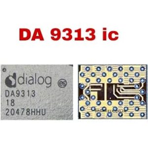
The DA9313 (originally developed by Dialog Semiconductor, now part of Renesas Electronics) is a high-performance, high-voltage power converter IC. It is most commonly found in high-end mobile devices (like the OPPO R17 Pro, Find X3, and Vivo IQOO 7) as a “switched capacitor divider” or “direct charger.” DA9313 Mobile Phone IC
Its primary claim to fame is its 98% efficiency, which allows for ultra-fast charging with minimal heat generation by halving the input voltage (e.g., converting 10V from a charger to 5V for the battery) without using bulky inductors. DA9313 Mobile Phone IC
DA9313 Technical Specifications
| Category | Parameter | Specification / Value |
| Basic Info | Manufacturer | Renesas Electronics (formerly Dialog Semi) |
| IC Function | High Efficiency Dual Cell Switched Cap Divider | |
| Typical Application | Smartphone Direct Charging / 2S Battery Power | |
| Electrical | Input Voltage ($V_{IN}$) | 5.0 V to 10.5 V |
| Output Voltage ($V_{OUT}$) | $\frac{1}{2} V_{IN}$ (Voltage Divider Mode) | |
| Max Output Current | 10 A (Standalone) / 20 A (Master/Slave) | |
| Peak Efficiency | Up to 98% | |
| Quiescent Current | 55 µA (Standalone) / 70 µA (Master/Slave) | |
| Switching Frequency | ~6 MHz | |
| Protection | Safety Features | Over-Current, Over-Temperature, Over-Voltage |
| Soft Start | Programmable to limit inrush current | |
| Physical | Package Type | 43-pin WLCSP (Wafer Level Chip Scale) |
| Dimensions | 3.545 mm x 2.815 mm | |
| Operating Temp | -40°C to +85°C (Ambient) | |
| Interface | Control Bus | $I^2C$ Compatible Interface |
| GPIOs | 2 Configurable Ports (Power Good, Interrupts) |
Key Features and Functionality
1. Inductor-less Design
Unlike traditional Buck converters that rely on large inductors to step down voltage, the DA9313 uses a switched capacitor (charge pump) architecture. This significantly reduces the PCB footprint and allows for a “low profile” design, as the external components (capacitors) can be less than 1mm in height.
2. High Current Capability (10A – 20A)
In a standalone configuration, the DA9313 can deliver a massive 10A of current. For ultra-premium devices requiring even faster charging speeds (like 65W or 120W systems), two DA9313 chips can be linked in a Master/Slave configuration to provide up to 20A of output current.
3. Efficiency and Thermal Management
Heat is the enemy of fast charging. Because the DA9313 operates at 98% efficiency, very little energy is wasted as heat. This allows the phone to charge at high speeds without the “thermal throttling” that usually slows down charging when the device gets too warm.
Common Mobile Phone Applications
Technicians and engineers usually encounter the DA9313 in the following scenarios:
-
Fast Charging Repairs: If a phone supports high-voltage direct charging but only charges slowly or not at all, the DA9313 is often the culprit.
-
2S Battery Systems: Devices that use two battery cells in series (stacked) to achieve higher voltages (common in gaming phones and foldables) use this IC to manage the power conversion to the rest of the system’s 1S (single cell) components.
-
Compatible Models: Widely used in OPPO, Realme, Vivo, and OnePlus flagship series.
Pinout and Control
The IC utilizes a 43-ball WLCSP layout. Key pins include:
-
VIN / VOUT: High current power paths.
-
CFLY (C1P, C1N, etc.): Connections for the flying capacitors that perform the voltage division.
-
SCL/SDA: $I^2C$ lines for the system CPU to monitor the chip’s status and adjust parameters.
-
nONKEY / EN: Hardware enable pins to wake the chip from sleep.
More Products : https://gaffarmarketdelhi.com


