

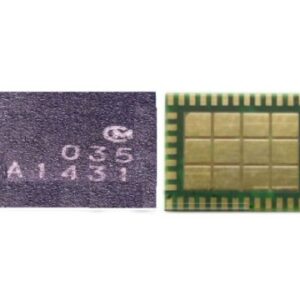
0.35 Mobile Phone IC
Optimized Performance for Mobile Devices
Our 0.35 Mobile Phone IC is engineered to provide superior performance for modern smartphones. Designed with precision, this high-quality IC ensures seamless device operation and improved efficiency. Whether for new builds or system upgrades, it’s the ultimate choice for reliable functionality. 0.35 Mobile Phone IC
Compact & Durable Design
With its compact build, the 0.35 Mobile Phone IC fits perfectly into even the most space-constrained devices. Manufactured using top-tier materials, it guarantees durability and long-lasting performance, making it a trusted solution for mobile phone manufacturers. 0.35 Mobile Phone IC
Versatile Application
The 0.35 Mobile Phone IC is suitable for a broad range of mobile phone models. Its adaptability ensures compatibility across various hardware configurations, delivering well-rounded performance without compromising quality. 0.35 Mobile Phone IC
In the context of mobile phone hardware, the term “0.35” typically refers to one of two critical physical metrics: the IC Package Pitch (the distance between solder balls on the chip) or the Process Technology Node ($0.35\text{ }\mu\text{m}$). 0.35 Mobile Phone IC
In modern smartphone repair and manufacturing, a 0.35mm pitch IC is an ultra-fine-pitch component (like Power Management ICs or Audio Codecs) designed for high-density motherboards. Below are the full technical specifications for a 0.35mm pitch Mobile IC. 0.35 Mobile Phone IC
0.35 Mobile IC Technical Specifications
| Feature | Specification Details |
| Component Category | Ultra-Fine Pitch Ball Grid Array (WLCSP/BGA) |
| Ball Pitch ($P$) | 0.35 mm (Center-to-center distance) |
| Solder Ball Diameter | $0.20\text{ mm} \pm 0.05\text{ mm}$ |
| Package Height | $0.35\text{ mm} – 0.60\text{ mm}$ (Ultra-low profile) |
| Substrate Material | Silicon (Wafer Level) or High-TG FR4 |
| Typical I/O Count | 30 to 120+ pins (High-density configuration) |
| PCB Trace Width | $\leq 0.05\text{ mm}$ (Requires HDI PCB technology) |
| Via Technology | Laser-drilled Microvias (Via-in-pad recommended) |
| Operating Temperature | $-40\text{°C}$ to $+125\text{°C}$ |
| Typical Applications | PMIC, Audio Amplifiers, RF Front-end, Sensors |
Core Architecture & Design
1. Mechanical Integration
The 0.35mm pitch is a standard for Wafer Level Chip Scale Packages (WLCSP). Unlike older 0.5mm or 0.8mm chips, these ICs have no plastic “housing.” The solder balls are attached directly to the silicon die. This allows the IC to be nearly the same size as the silicon itself, crucial for modern slim smartphones.
2. Thermal & Electrical Performance
-
High Speed: Shorter interconnects between the die and the PCB reduce parasitic inductance, improving signal integrity for 5G and high-frequency audio.
-
Heat Dissipation: Because the chip is mounted directly to the board, the PCB acts as a primary heatsink. Modern 0.35 ICs often use “ground balls” in the center of the array to pull heat away from the core logic. 0.35 Mobile Phone IC
3. Manufacturing Requirements
Implementing a 0.35mm pitch IC requires advanced Surface Mount Technology (SMT):
-
Solder Paste: Requires Type 5 or Type 6 solder paste (smaller grain size) to prevent bridging between the tiny contacts. 0.35 Mobile Phone IC
-
Stencil Design: Stencils must be laser-cut with an electro-polished finish, typically only $0.08\text{ mm}$ to $0.10\text{ mm}$ thick. 0.35 Mobile Phone IC
-
Placement Accuracy: High-precision pick-and-place machines with a tolerance of $\pm 25\text{ }\mu\text{m}$ are mandatory.
Common Mobile IC Variants (0.35mm)
Mobile technicians frequently encounter “0.35” specifications in these specific modules:
Power Management (PMIC)
These ICs manage battery charging and voltage distribution. They use the 0.35mm pitch to pack hundreds of power rails into a space smaller than a fingernail.
-
Voltage Range: $1.8\text{V}$ to $5.5\text{V}$ input.
-
Efficiency: Typically $>90\%$ for Buck converters.
RF Front-End / Power Amplifiers
Used for signal processing in Samsung, iPhone, and Xiaomi devices. These often carry the “035” or “0.35” designation in repair manuals to indicate the reballing stencil size needed.
-
Frequency Support: $700\text{ MHz}$ to $6\text{ GHz}$ (Sub-6 5G).
Repair & Maintenance Data
For technicians performing “reballing” or IC replacement, the following parameters are critical:
Note: Excessive heat during desoldering can delaminate the ultra-thin 0.35mm substrate. Always use a pre-heater.
-
Desoldering Temp: $330\text{°C} – 350\text{°C}$ (Airflow: 30-40%).
-
Reballing Stencil: 0.35mm Universal BGA Stencil (0.12mm thickness).
-
Solder Ball Size: $0.2\text{ mm}$ or $0.25\text{ mm}$ leaded/lead-free spheres.
More Products : https://gaffarmarketdelhi.com


