

58083-11 Mobile Phone IC
Optimized Performance for Mobile Devices
The 58083-11 Mobile Phone IC Integrated Circuit is designed to enhance the efficiency and functionality of modern smartphones. Engineered for durability and high-speed performance, this IC ensures seamless operation even under heavy usage. 58083-11 Mobile Phone IC
Compact and Reliable Design
Designed with precision and compactness in mind, the 58083-11 Mobile Phone IC occupies minimal space while delivering maximum performance. Its robust design is perfect for smartphones requiring dependable and efficient components. 58083-11 Mobile Phone IC
Versatile Integration
With compatibility across multiple smartphone models, the 58083-11 Mobile Phone IC is a versatile choice for manufacturers and repair technicians. Its easy integration ensures smooth functionality and faster implementation, saving time and effort. 58083-11 Mobile Phone IC
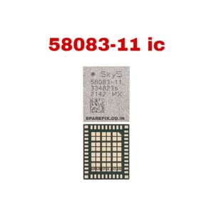
The 58083-11 (commonly identified as the SKY58083-11) is a sophisticated RF Front-End Module (FEM) manufactured by Skyworks Solutions. It is a critical component in modern 5G smartphones, serving as a Power Amplifier Module with Integrated Duplexers (PAMiD). 58083-11 Mobile Phone IC
This IC is primarily responsible for the transmission and reception of signals in the low-frequency bands, ensuring your phone can maintain a stable connection to cell towers even in areas with weak signal strength. 58083-11 Mobile Phone IC
Technical Specifications Table
| Feature | Specification Details |
| Manufacturer | Skyworks Solutions Inc. |
| Model Number | SKY58083-11 (often shortened to 58083-11) |
| Component Type | RF Front-End Module (FEM) / PAMiD |
| Technology Support | 2G (GSM), 3G (WCDMA), 4G (LTE), 5G (NR) |
| Frequency Bands | Quad-band GSM; Low-Band (LB) 3G/4G/5G |
| Package Type | LGA (Land Grid Array) / MCM (Multi-Chip Module) |
| Pin/Pad Count | 46-pad / 56-pad (configuration varies by batch/revision) |
| Operating Voltage | 3.4V to 5V (standard for mobile RF PAs) |
| Control Interface | MIPI RFFE (Radio Frequency Front End) 2.1/3.0 |
| Package Dimensions | Approx. 7.6 mm x 6.0 mm x 0.7 mm |
| Integration | PA, LNA, RF Switches, RFFE Controller, SAW Duplexers |
Core Functions and Internal Architecture
The 58083-11 is not just a single transistor; it is a “multi-die” module. Think of it as a tiny city within a single chip. Its internal architecture includes:
-
Power Amplifier (PA): The “voice” of your phone. It boosts low-power signals from the modem so they are strong enough to reach a cell tower miles away. 58083-11 Mobile Phone IC
-
Low Noise Amplifier (LNA): The “ears” of your phone. It amplifies the extremely faint signals received from the tower without adding background static. 58083-11 Mobile Phone IC
-
RF Switches: These act like traffic cops, routing signals between the antenna and the appropriate internal path (transmit vs. receive).
-
SAW Duplexers: These filters allow the phone to send and receive data at the same time on the same antenna without the two signals interfering with each other.
Device Compatibility
This IC is widely used in flagship and mid-range devices that require high-efficiency 5G connectivity. It is a staple in the Samsung ecosystem and several other high-end manufacturers.
Popular Models Using 58083-11:
-
Samsung Galaxy S22 Ultra (Global and US variants)
-
Samsung Galaxy A53 5G (Model SM-A536)
-
Samsung Galaxy A33 5G
-
Samsung Galaxy A54 5G
Signs of a Failing 58083-11 IC
In the repair industry, this IC is a frequent culprit for network-related failures. Because it handles the “Low Band” frequencies, a fault in this chip usually results in specific symptoms:
-
“No Service” or “Searching” constantly, even in known good areas.
-
Emergency Calls Only: The phone can see the network but cannot “handshake” to authenticate.
-
Greyed-out Network Settings: Occasionally, a short circuit within the IC can cause the modem firmware to crash or become unresponsive.
-
High Battery Drain: If the PA is damaged but not dead, it may draw excessive current (leakage), causing the phone to run hot and the battery to drain rapidly.
Installation and Repair Notes
Note: This is a BGA (Ball Grid Array) component. It is soldered to the motherboard using tiny solder balls underneath the chip.
-
Skill Level: Professional. This requires a microscope, high-quality flux, and a hot-air rework station.
-
Temperature Profile: Most technicians recommend a reflow temperature of approximately 230°C to 250°C depending on the lead-free solder used, though the chip itself can withstand higher bursts during the soldering process.
-
Orientation: The “Pin 1” marker (usually a small dot on the corner of the IC) must align perfectly with the marking on the motherboard.
Official Website : https://gaffarmarketdelhi.com


