O31 Mobile Phone IC
Reliable and Efficient Integrated Circuit
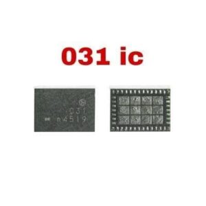
The O31 Mobile Phone IC is a cutting-edge solution designed to optimize performance and ensure seamless device functionality. Whether you’re upgrading or repairing your mobile device, this IC is engineered for reliability and efficiency. O31 Mobile Phone IC
Enhanced Connectivity and Durability
Built with advanced technology, the O31 Mobile Phone IC ensures smooth connectivity and robust performance. Its durable design makes it a perfect choice for both daily use and long-term support in modern mobile phones. O31 Mobile Phone IC
Perfect Choice for Mobile Optimization
Designed to meet the demanding needs of mobile devices, the O31 delivers superior efficiency, reduced power consumption, and enhanced compatibility. Elevate your device’s performance with this essential component crafted for excellence. O31 Mobile Phone IC
In the mobile repair and RF engineering industry, the O31 IC (often labeled as O31 P1891 or 031) refers to a specific Power Amplifier (PA) IC commonly utilized in high-frequency signal processing. This component is primarily associated with Samsung devices (notably the Galaxy A710 series) and various high-performance LTE/5G handsets. O31 Mobile Phone IC
Below is the comprehensive technical breakdown and specification for the O31 Power Amplifier IC. O31 Mobile Phone IC
1. Technical Overview
The O31 is a Multi-Mode Multi-Band (MMMB) Power Amplifier. Its primary function is to amplify low-power RF signals from the transceiver to a level sufficient for transmission via the antenna while maintaining high linearity and efficiency. O31 Mobile Phone IC
| Feature | Specification |
| Component Name | O31 / 031 P1891 |
| Component Category | Power Amplifier Module (PAM) |
| Technology | GaAs HBT (Heterojunction Bipolar Transistor) |
| Primary Function | Uplink Signal Amplification (TX) |
| Package Type | LGA (Land Grid Array) |
| Control Interface | MIPI RFFE (Radio Frequency Front End) |
| Standard Support | WCDMA, LTE-FDD, LTE-TDD, 5G NR |
2. Electrical Characteristics
The O31 IC operates within strict electrical parameters to ensure the longevity of the RF front-end.
Operating Voltage & Power
| Parameter | Symbol | Min | Typ | Max | Unit |
| Supply Voltage | $V_{CC}$ | 0.5 | 3.4 | 4.8 | V |
| Battery Voltage | $V_{BATT}$ | 3.0 | 3.8 | 5.0 | V |
| Digital I/O Voltage | $V_{IO}$ | 1.65 | 1.8 | 1.95 | V |
| Quiescent Current | $I_{CQ}$ | — | 15 | 25 | mA |
| Max Output Power | $P_{OUT}$ | — | 28.5 | 30.0 | dBm |
3. Frequency Band Support
The O31 IC is a versatile module designed for “Global” band coverage, particularly focusing on Mid and High bands (MH).
| Band Category | Frequency Range | Supported Standards |
| Mid Bands | 1710 MHz – 2020 MHz | LTE B1, B2, B3, B4, B25, B39 |
| High Bands | 2300 MHz – 2690 MHz | LTE B7, B30, B38, B40, B41 |
| 5G NR | 2.5 GHz Range | n41, n77 (partial support) |
4. Performance Specifications
The efficiency of the O31 is vital for maintaining the battery life of the mobile device. It is typically optimized for Average Power Tracking (APT).
| Performance Metric | Detail |
| Power Added Efficiency (PAE) | Up to 45% (LTE QPSK) |
| Gain (High Power Mode) | 28 dB to 31 dB |
| Gain (Low Power Mode) | 10 dB to 14 dB |
| Input Return Loss | < -10 dB |
| Harmonic Suppression | 2nd Harmonic: < -35 dBc / 3rd Harmonic: < -40 dBc |
5. Pin Configuration & Mechanical Specs
The O31 uses a high-density LGA package designed for superior thermal dissipation.
| Detail | Measurement / Type |
| Dimensions | Approx. 4.0 mm x 6.5 mm |
| Height | 0.75 mm (Ultra-thin) |
| Pin Count | 42-Pad Layout |
| Solder Ball/Pad Material | Lead-Free (RoHS Compliant) |
| Thermal Pad | Central ground pads required for heat syncing |
6. Functional Block Description
The O31 IC is not a single transistor but a complex system-in-package (SiP) containing:
-
Power Amplifier Core: Two to three separate GaAs stages for different frequency ranges.
-
Directional Coupler: Integrated to monitor output power and provide feedback to the transceiver.
-
Digital Controller: A CMOS-based logic block that decodes MIPI RFFE commands to switch between bands and gain modes.
-
Matching Network: Internal $50 \Omega$ matching to minimize the need for external inductors and capacitors.
7. Troubleshooting & Repair Tips
If a mobile device shows “No Service” or “Emergency Calls Only” despite a detected SIM card, the O31 IC is a common suspect.
-
Heat Sensitivity: During reballing or replacement, the IC should not exceed 260°C for more than 10 seconds. Excessive heat will delaminate the GaAs substrate.
-
Voltage Check: Ensure $V_{CC}$ (usually from the Power Management IC or a dedicated Boost DC-DC) is reaching the IC during a call attempt.
-
MIPI RFFE Clock/Data: If the IC does not “wake up,” check the MIPI RFFE bus for continuity to the CPU/Transceiver.
Note: The O31 IC is often interchangeable with specific versions of the Vanchip VC7643-63 or Skyworks Sky-series depending on the PCB revision, but always verify the exact part suffix before installation.
More Products : https://gaffarmarketdelhi.com