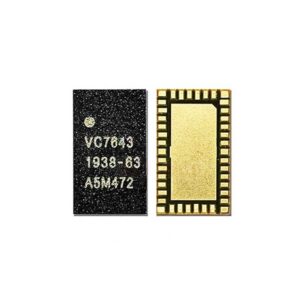
VC7643 63 Mobile Phone IC
The VC7643 63 Mobile Phone IC is a high-performance, Multi-Mode Multi-Band (MMMB) Power Amplifier Module (PAM) manufactured by Vanchip Technologies. It is a mission-critical component in the radio frequency (RF) front-end of 4G LTE and 5G NR smartphones, responsible for amplifying low-power signals to the levels required for transmission to cellular towers. VC7643 63 Mobile Phone IC
As an “MMMB” module, it is designed to handle a vast array of frequency bands, simplifying the hardware design for manufacturers who need their phones to work on different carriers worldwide. VC7643 63 Mobile Phone IC
1. General Device Overview
The VC7643-63 serves as the “powerhouse” of the mobile transmit chain. It integrates multiple power amplifier dies, RF switches, and a digital controller into a single compact package. VC7643 63 Mobile Phone IC
| Feature | Specification Details |
| Manufacturer | Vanchip Technologies Ltd. |
| Part Number | VC7643-63 |
| Device Type | Multi-Mode Multi-Band Power Amplifier Module (MMMB PAM) |
| Supported Generations | 3G (WCDMA/HSPA), 4G (LTE), 5G (NR Sub-6GHz) |
| Process Technology | GaAs HBT (Power Amplifier), CMOS (Digital Controller), SOI (Switch) |
| Package Dimensions | 4.0 mm x 6.8 mm x 0.704 mm |
| Lead Count | 42-Pad LGA (Land Grid Array) |
| Digital Interface | MIPI RFFE 2.1 (Radio Frequency Front End) |
2. Electrical Specifications
These parameters define the safe operating limits and power requirements for the IC. Operating the device outside these ranges can lead to permanent damage. VC7643 63 Mobile Phone IC
Absolute Maximum Ratings
| Parameter | Symbol | Min | Max | Unit |
| Battery Supply Voltage | $V_{BATT}$ | -1.2 | 6.0 | V |
| Supply Voltage (VCC) | $V_{CC1}, V_{CC2}$ | -0.5 | 6.0 | V |
| MIPI Supply Voltage | $V_{IO}$ | — | 2.0 | V |
| RF Input Power | $P_{IN}$ | — | 10 | dBm |
| ESD Protection (HBM) | $ESD_{HBM}$ | -1.0 | +1.0 | kV |
| ESD Protection (CDM) | $ESD_{CDM}$ | -1.0 | +1.0 | kV |
| Storage Temperature | $T_{STG}$ | -40 | +150 | °C |
Recommended Operating Conditions
| Parameter | Symbol | Min | Typ | Max | Unit |
| Primary Supply Voltage | $V_{CC}$ | 0.55 | 3.4 | 4.8 | V |
| Battery Voltage | $V_{BATT}$ | 3.2 | 3.4 | 4.8 | V |
| I/O Digital Voltage | $V_{IO}$ | 1.65 | 1.8 | 1.95 | V |
| MIPI Clock Frequency | $F_{SCLK}$ | — | 26 | 52 | MHz |
| Operating Temperature | $T_{CASE}$ | -30 | +25 | +100 | °C |
3. Frequency Band & Modulation Support
The VC7643-63 is versatile, covering nearly all major cellular frequencies from 663 MHz to 2.7 GHz.
Cellular Bands Covered
-
5G NR Bands: n1, n2, n3, n5, n7, n8, n12, n20, n25, n28, n38, n40, n41, n66, n71.
-
4G LTE FDD/TDD: Bands 1, 2, 3, 4, 5, 7, 8, 12, 13, 17, 20, 25, 26, 28, 30, 34, 38, 39, 40, 41, 66, 71.
-
3G WCDMA/HSPA: Bands 1, 2, 3, 4, 5, 8, 9.
-
Legacy Support: CDMA BC0, BC1, BC4, BC6, BC10, BC15; TD-SCDMA Bands 34, 39.
Modulation & Data Capability
| Waveform / Modulation | Supported Configurations |
| Uplink Modulations | QPSK, 16QAM, 64QAM, 256QAM (NR) |
| LTE Bandwidths | 1.4, 3, 5, 10, 15, 20 MHz |
| 5G NR Bandwidths | 5, 10, 15, 20, 40, 60, 80, 100 MHz |
| Special Support | LTE HPUE (High Power User Equipment) Power Class 2 |
| Carrier Aggregation | Intra-Band CA support for Bands 3, 39, 40, 41 |
4. Key Functional Features
-
Internal RF Matching: The RF input and output ports are internally matched to $50\Omega$, removing the need for complex external tuning circuits and saving PCB space.
-
Integrated DC-Block: Output ports include internal DC-blocking capacitors, further reducing component count.
-
Efficiency Optimization: Fully optimized for operation with DC-DC Converters (Average Power Tracking or Envelope Tracking) to maximize battery life.
-
Gain Modes: Supports High and Low Gain modes to maintain high linearity and low noise at different power levels.
-
Digital Control: Uses the MIPI RFFE 2.1 standard for fast, reliable communication with the phone’s baseband processor.
5. Device Compatibility & Applications
Because of its high integration and broad band support, the VC7643-63 is found in many popular mid-range and flagship smartphones.
| Manufacturer | Notable Models Using VC7643-63 |
| Oppo | Oppo A32, A52, A72, Reno 10 5G |
| Xiaomi | Mi 13 Pro, Redmi 9A |
| Vivo | Vivo X90 Pro 5G |
| Realme | Realme 11 5G, 11X 5G |
| General | TDD/FDD Multiband Handsets, LTE Data Cards |
6. Technical Maintenance & Handling
Caution: The VC7643-63 is an LGA package sensitive to Electrostatic Discharge (ESD) and Moisture (MSL 3). Repair or replacement requires:
A high-precision hot air rework station.
BGA reballing stencils specifically for the 42-pad layout.
Proper pre-heating of the PCB to avoid thermal stress on neighboring components like the CPU or Power Management IC (PMIC).
4. Key Functional Features
Internal RF Matching: The RF input and output ports are internally matched to $50\Omega$, removing the need for complex external tuning circuits and saving PCB space.
Integrated DC-Block: Output ports include internal DC-blocking capacitors, further reducing component count.
Efficiency Optimization: Fully optimized for operation with DC-DC Converters (Average Power Tracking or Envelope Tracking) to maximize battery life.
Gain Modes: Supports High and Low Gain modes to maintain high linearity and low noise at different power levels.
Digital Control: Uses the MIPI RFFE 2.1 standard for fast, reliable communication with the phone’s baseband processor.
More Products https://gaffarmarketdelhi.com