

BQ 25601 Original Mobile Phone IC
Reliable Performance for Mobile Devices
The BQ 25601 Original Mobile Phone IC is a premium integrated circuit designed for seamless smartphone functionality. Engineered for efficiency, it ensures optimal performance across a variety of mobile platforms, making it the ideal choice for manufacturers and repair professionals alike. BQ 25601 Original Mobile Phone IC
Quality That You Can Trust
Crafted with precision and attention to detail, the BQ 25601 IC guarantees durability and reliability. Its original design ensures consistent results, enabling your mobile devices to perform at their peak. Say goodbye to compatibility issues and enjoy a component that integrates effortlessly with your system. BQ 25601 Original Mobile Phone IC
Perfect Fit for Your Repair Needs
Whether you’re upgrading or repairing, the BQ 25601 Original Mobile Phone IC is the perfect fit for your needs. With consistent performance and superior build quality, this IC supports smooth device operations, giving you peace of mind and unparalleled functionality. BQ 25601 Original Mobile Phone IC
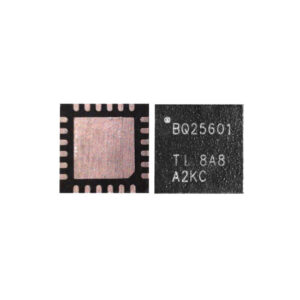
The BQ25601 is a high-performance, $I^2C$ controlled 3-A switch-mode battery charge management and system power path management device. Developed by Texas Instruments, it is a critical component in modern mobile phones (like the Redmi Note 5A, Huawei P Smart Z, and Samsung A31) because it balances fast charging with advanced thermal and safety protections. BQ 25601 Original Mobile Phone IC
Core Technical Specifications
| Feature | Specification Details |
| Manufacturer | Texas Instruments (TI) |
| Charge Current | Up to 3.0 A (Programmable) |
| Input Voltage Range | 3.9 V to 13.5 V (Operating) |
| Max Input Voltage | 22 V (Absolute Maximum Rating) |
| Switching Frequency | 1.5 MHz (High-efficiency Buck converter) |
| Efficiency | 92% at 2-A from 5-V input |
| OTG Boost Output | 5.15 V @ 1.2 A (92% efficiency at 1-A) |
| Communication | $I^2C$ Interface (up to 400 kbps) |
| Voltage Accuracy | ±0.5% Charge Voltage Regulation |
| Current Accuracy | ±5% at 1.5-A Charge Current |
| Package Type | 24-Pin WQFN ($4.0 \text{ mm} \times 4.0 \text{ mm}$) |
| Quiescent Current | 17 µA (Battery leakage in ship mode) |
Key Operational Features
1. Narrow VDC (NVDC) Power Path Management
The BQ25601 uses NVDC architecture, which is essential for mobile devices. It allows the system (phone) to start up instantly even if the battery is deeply discharged or completely missing. The IC prioritizes the system load; if the input power is limited, it reduces the charging current to ensure the phone stays on. BQ 25601 Original Mobile Phone IC
2. Advanced Charging Profile
The IC manages the battery life cycle through three distinct phases:
-
Pre-conditioning: Gently wakes up a “dead” battery.
-
Constant Current (CC): The fast-charging phase where the 3-A current is applied.
-
Constant Voltage (CV): Topping off the battery safely as it reaches full capacity. BQ 25601 Original Mobile Phone IC
3. USB Integration and OTG
It supports USB On-The-Go (OTG), meaning the phone can act as a power bank to charge other devices. It can boost the battery voltage to 5.15 V to power external USB peripherals with high efficiency.
Safety and Protection Mechanisms
Mobile safety is a priority for the BQ25601. It includes several hardware-level safeguards:
-
Thermal Regulation: Automatically reduces charging current if the internal temperature reaches 110°C or 120°C.
-
Input Over-Voltage Protection (OVP): Protects the internal circuitry if a faulty high-voltage charger (up to 22V) is plugged in.
-
JEITA Monitoring: Uses the TS pin to monitor the battery’s temperature via a thermistor, stopping charging if the battery is too cold or too hot.
-
Watchdog Timer: If the phone’s software hangs, the IC resets to safe default charging values.
Troubleshooting & Common Faults
In the mobile repair industry, the BQ25601 is often replaced when a phone shows the following symptoms:
-
Fake Charging: The charging icon is visible, but the percentage never increases.
-
No Detection: The phone does not react to a USB cable being plugged in.
-
Short Circuit: The device is “dead” due to a short on the VCC_MAIN or SYS rail, which this IC manages.
-
Boot Loop: If the REGN pin (internal regulator) is not outputting approximately 6.0 V, the IC is likely faulty.
More Products : https://gaffarmarketdelhi.com


