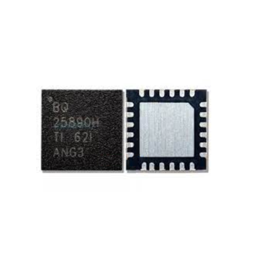
BQ 25890H Mobile Phone IC
Introducing the BQ 25890H Mobile Phone IC
The BQ 25890H Mobile Phone IC is a highly efficient, integrated charging solution designed to optimize power management in modern mobile devices. Engineered with advanced features, this IC delivers precise charging performance, ensuring your devices stay powered up with maximum efficiency. BQ 25890H Mobile Phone IC
Reliability and Precision
Designed for reliability, the BQ 25890H comes with cutting-edge thermal management and overcurrent protection. Its consistent charge control ensures prolonged battery health without compromising performance. This IC is the perfect choice for manufacturers and developers focused on delivering durable and high-quality electronic solutions. BQ 25890H Mobile Phone IC
Perfect for Mobile Applications
The BQ 25890H IC’s compact design and versatile functionality make it an ideal fit for various smartphone and portable device applications. Whether you’re building the next innovative gadget or upgrading existing hardware, this IC seamlessly integrates into your design, helping you achieve superior power efficiency without adding complexity.
The BQ25890H is a highly integrated, 5-A switch-mode battery charge management and system power path management device for single-cell Li-Ion and Li-polymer batteries. It is part of the MaxCharge™ technology family from Texas Instruments, designed specifically for high-input voltage fast charging and USB On-the-Go (OTG) applications.
Compared to the standard BQ25890, the “H” version includes an enhanced programmable D+/D– driver, allowing the device to handshake with various high-voltage adjustable adapters (HVDCP) commonly found in the market.
BQ25890H Full Technical Specifications
| Feature | Detailed Specification |
| Manufacturer | Texas Instruments (TI) |
| Technology | MaxCharge™ Technology (Fast Charging) |
| Max Charge Current | 5.0 A |
| Operating Input Voltage | 3.9 V to 14.0 V |
| Absolute Max Input Voltage | 22 V |
| Charge Efficiency | 93% at 2A / 91% at 3A (with 9V/12V input) |
| Switching Frequency | 1.5 MHz |
| ADC Integration | 7-Channel (Voltage, Temp, Current Monitoring) |
| Power Path Management | Narrow VDC (NVDC) Architecture |
| OTG Output Voltage | 4.5 V to 5.5 V (Adjustable) |
| OTG Output Current | Up to 2.4 A |
| Quiescent Current | 12 µA (Ship Mode) |
| Package Type | 24-Pin WQFN (4.0 mm × 4.0 mm) |
| Communication Interface | $I^2C$ Controlled (up to 400 kHz) |
Detailed Functional Overview
1. High-Efficiency Buck Charger
The BQ25890H operates as a high-frequency synchronous switch-mode buck charger. By running at 1.5 MHz, it allows the use of small, low-profile inductors (typically $1.0\text{ }\mu\text{H}$ or $1.5\text{ }\mu\text{H}$), which is critical for the slim design of modern smartphones. It is optimized for high-voltage inputs ($9\text{V}$ and $12\text{V}$), maintaining over 90% efficiency even at high charging currents.
2. Narrow VDC (NVDC) Power Path
The NVDC architecture is a significant upgrade over traditional power paths. In this system:
-
The system (phone motherboard) is powered directly from the input if the battery is depleted or missing. BQ 25890H Mobile Phone IC
-
The system voltage is regulated slightly above the battery voltage but never drops below the minimum system voltage ($3.5\text{V}$ default). BQ 25890H Mobile Phone IC
-
This allows a “Dead Battery” phone to turn on instantly as soon as the charger is plugged in. BQ 25890H Mobile Phone IC
3. Programmable D+/D– Handshaking
The key differentiator for the BQ25890H is its ability to communicate with high-voltage adapters. It can simulate various handshake protocols to tell the wall adapter to increase its output from $5\text{V}$ to $9\text{V}$ or $12\text{V}$, enabling the “Fast Charge” or “Quick Charge” features seen in Android devices. BQ 25890H Mobile Phone IC
4. Integrated 7-Channel ADC
The IC contains a built-in Analog-to-Digital Converter (ADC) that provides high-accuracy monitoring of:
-
VBUS: Input voltage.
-
VBAT: Battery voltage.
-
ICHG: Charge current.
-
TS: Battery temperature (using a thermistor).
-
TDIE: Internal IC temperature.
Pin Configuration & Troubleshooting
| Pin Name | Pin Number | Function / Technical Note |
| VBUS | 1 | Input power connection. Check for $5\text{V}/9\text{V}$ here. |
| D+ / D- | 2, 3 | Data lines for charger detection and handshaking. |
| STAT | 4 | Open-drain output indicating charge status (Blinking = Fault). |
| SDA / SCL | 5, 6 | $I^2C$ interface for CPU communication. |
| OTG | 7 | High = Enable Boost Mode for USB-OTG power output. |
| ILIM | 10 | Hardware-based input current limit (via resistor to GND). |
| TS | 11 | Temperature Sense. If battery temp is high, charging stops. |
| BAT | 13, 14 | Battery connection. Measures battery voltage. |
| SYS | 15, 16 | System output. Powers the phone’s motherboard. |
| REGN | 22 | Internal LDO ($6\text{V}$). Essential for driving internal FETs. |
Common Issues in Mobile Repair
In smartphone repair, the BQ25890H is often replaced when the following symptoms occur:
-
Fake Charging: The phone shows a charging icon but the battery percentage does not increase. This often happens if the internal MOSFETs or the sensing logic inside the IC fail.
-
No Detection: The phone does not react to the charger at all. Technicians should measure the voltage at the VBUS pin ($5\text{V}$) and then at the REGN pin ($6\text{V}$). If VBUS is present but REGN is $0\text{V}$, the IC is likely defective.
-
Overheating: If the area near the charging inductor gets extremely hot, it may indicate a short within the BQ25890H.
-
Slow Charging: If the phone only charges at $450\text{mA}$ despite using a fast charger, the D+/D– handshaking logic inside the IC may be damaged.
Comparison: BQ25890 vs. BQ25890H
| Feature | BQ25890 | BQ25890H |
| D+/D- Detection | Standard (BC1.2) | Programmable Driver |
| HVDCP Support | Limited | Full Support |
| Application | Standard Fast Charge | Adjustable Voltage Fast Charge |

More Products : https://gaffarmarketdelhi.com