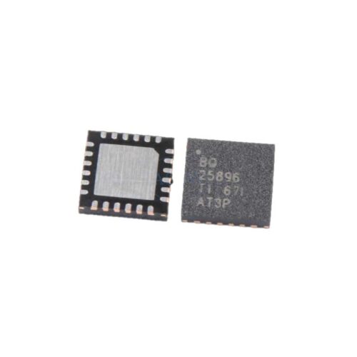
BQ 25896 Original Mobile Phone IC
Premium Quality Mobile Phone IC
The BQ 25896 Original Mobile Phone IC offers top-notch reliability and performance, designed to meet the demands of modern mobile devices. It ensures seamless power management and efficient operation, making it an essential component for your mobile solutions. BQ 25896 Original Mobile Phone IC
Optimized for Performance
Engineered to deliver exceptional results, this IC supports advanced charging capabilities while enhancing device stability. With its original design and cutting-edge technology, the BQ 25896 guarantees optimal compatibility with a wide range of mobile phone models, ensuring a hassle-free integration process. BQ 25896 Original Mobile Phone IC
Why Choose the BQ 25896?
Whether you’re repairing or manufacturing mobile devices, this IC is your reliable partner for quality and durability. Its original construction ensures long-term performance, helping you stay ahead in delivering premium-grade mobile technologies to your customers. BQ 25896 Original Mobile Phone IC
The BQ25896 is a highly sophisticated, $I^2C$ controlled, 3-A single-cell switch-mode battery charger featuring MaxCharge™ technology. It is designed for high-input voltage fast charging and is widely used in flagship and mid-range smartphones (such as those from Xiaomi, Meizu, and Huawei) due to its ability to handle up to $14\text{V}$ inputs.
Below is the comprehensive technical breakdown and full specifications for the BQ25896 IC.
1. Technical Specifications Table
| Parameter | Specification Details |
| Manufacturer | Texas Instruments (TI) |
| Input Voltage Range | 3.9 V to 14 V (Operating) |
| Absolute Max Voltage | 22 V (VBUS Pin) |
| Max Charge Current | 3.0 A (Programmable via $I^2C$) |
| Charge Efficiency | 92.5% @ 2A / 90.5% @ 3A |
| OTG Output (Boost) | Adjustable 4.5 V to 5.5 V @ 2.0 A |
| Boost Efficiency | 93% at 5V / 1A |
| Switching Frequency | 1.5 MHz (Buck) / 500 kHz or 1.5 MHz (Boost) |
| Voltage Regulation | ±0.5% Accuracy |
| Integrated ADC | 7-bit (Monitors Voltage, Current, Temperature) |
| Standby Current | < 12 µA (Ship Mode) |
| Package | 24-Pin WQFN ($4.0 \text{ mm} \times 4.0 \text{ mm}$) |
2. Pin Configuration and Functions
For hardware troubleshooting and motherboard tracing, understanding the pinout is essential.
-
VBUS (Pin 24): Primary input source. It detects the charger type (USB, High Voltage, etc.).
-
SW (Switching Node): Connects to the inductor. This is where the voltage is “stepped down” during charging and “stepped up” during OTG mode.
-
SYS (System Rail): Provides power to the phone’s internal components. The NVDC management keeps this rail above $3.5\text{V}$ even if the battery is dead.
-
BAT (Battery Connection): Direct path to the Li-ion cell.
-
REGN (Pin 22): An internal $6\text{V}$ LDO output used to power the internal gate drivers. If this voltage is missing, the IC is dead.
-
SDA/SCL: Data and Clock lines for $I^2C$ communication with the CPU.
-
TS (Temperature Sense): Connects to the battery’s thermistor to monitor for overheating.
3. Core Technologies & Features
MaxCharge™ and Fast Charging
The BQ25896 is optimized for High Voltage Fast Charging. Unlike standard chargers limited to $5\text{V}$, this IC can accept $9\text{V}$ or $12\text{V}$ from a fast charger, converting it efficiently to battery voltage with minimal heat. This reduces charging time by up to 50% compared to traditional 2-A chargers.
Input Current Optimizer (ICO)
This is a proprietary TI technology that prevents the phone from “crashing” a weak charger. The IC automatically detects the maximum power a charger can provide without the voltage dropping. This ensures maximum charging speed regardless of whether you use a high-quality original adapter or a cheaper third-party one.
Integrated 7-bit ADC
The inclusion of an Analog-to-Digital Converter (ADC) allows the phone’s operating system to read real-time data directly from the IC. This includes:
-
VBUS (Input) voltage.
-
Battery voltage and charge current.
-
System temperature.
-
Input current limit status.
4. Troubleshooting and Common Faults
In mobile repair shops, the BQ25896 is a common replacement part. Here are the symptoms of failure and how to diagnose them:
A. Fake Charging
The phone shows the charging symbol but the battery percentage never increases. This is often caused by a failure in the ICO algorithm or a damaged internal BATFET.
-
Check: Measure the voltage at the BAT pin. If it is lower than $3.7\text{V}$ while plugged in, the IC is likely not pushing current. BQ 25896 Original Mobile Phone IC
B. No USB Detection / Slow Charging
If the $I^2C$ lines (SDA/SCL) are pulled low or the internal detection circuit is fried, the phone will default to a “slow charge” mode ($500\text{mA}$). BQ 25896 Original Mobile Phone IC
-
Check: Use an oscilloscope to check for data pulses on the SDA/SCL lines. BQ 25896 Original Mobile Phone IC
C. Dead Phone (Short Circuit)
If the phone is completely dead and the DC Power Supply shows a high current draw (short circuit), the BQ25896 might have an internal short between VBUS and GND. BQ 25896 Original Mobile Phone IC
-
Check: Measure the resistance to ground on the VBUS and SYS capacitors. BQ 25896 Original Mobile Phone IC
D. OTG Failures
If the phone cannot detect a mouse, keyboard, or flash drive, the Boost Converter within the BQ25896 may be faulty.
-
Check: Enable OTG in settings and check for $5\text{V}$ at the USB port (VBUS).
5. Summary for Technicians
The BQ25896 is an “intelligent” charger. Replacing it requires a high-quality Hot Air Station (set to approx. $350^\circ\text{C}$ to $380^\circ\text{C}$) because the center thermal pad is soldered to the ground plane, which acts as a large heat sink. Always ensure the REGN capacitor ($6\text{V}$) is present and functional, as many “charging issues” are actually caused by a tiny cracked capacitor near this pin rather than the IC itself.

More Products : https://gaffarmarketdelhi.com