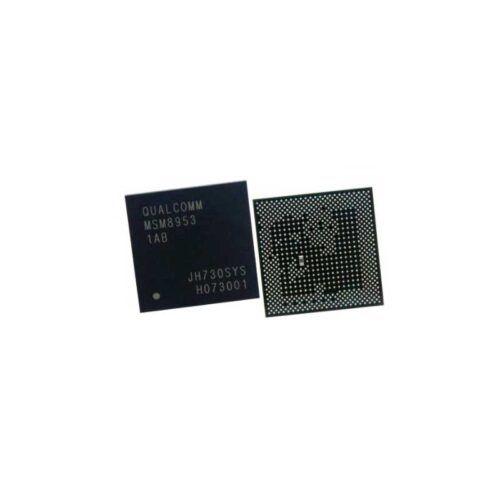
MSM 8953 1A3B CPU Mobile Phone IC
Unleashing Efficiency with MSM 8953 1A3B CPU
The MSM 8953 1A3B CPU Mobile Phone IC is designed to deliver unmatched efficiency and reliability for today’s demanding mobile devices. With its advanced architecture and focus on performance optimization, this IC ensures seamless operations across various applications, from routine mobile phone tasks to high-end processing requirements. MSM 8953 1A3B CPU Mobile Phone IC
Exceptional Performance Meets Cutting-edge Technology
This mobile phone IC is crafted with precision, utilizing state-of-the-art technology to meet modern requirements. The MSM 8953 1A3B CPU supports high-speed processing and integrates seamlessly into existing device architectures, making it ideal for manufacturers aiming to enhance both efficiency and user experience. MSM 8953 1A3B CPU Mobile Phone IC
Key features include robust thermal management, superior power efficiency, and compatibility with high-performance memory configurations. These attributes contribute to smoother multitasking, faster application responsiveness, and longer device uptime, placing it among the best choices for mobile phone development. MSM 8953 1A3B CPU Mobile Phone IC
Your Go-to Solution for Enhanced Mobile Device Performance
Whether you’re a manufacturer, designer, or developer, the MSM 8953 1A3B CPU Mobile Phone IC offers the reliability you need in a compact, high-functioning package. Its adaptability and efficiency cater to a wide range of mobile devices, providing consistent performance without compromising quality.
By choosing the MSM 8953 1A3B CPU IC, you invest in a solution designed to enhance every aspect of device functionality—from processing speeds to energy management—ensuring your devices stand out in highly competitive consumer markets.
The MSM8953, commercially known as the Qualcomm Snapdragon 625, is a landmark System-on-Chip (SoC) in the mobile industry. The “1A3B” suffix typically refers to specific part numbering related to the physical packaging, revision, or binning of the Integrated Circuit (IC).
Introduced as part of Qualcomm’s 600-series, this IC was a game-changer because it was the first in its class to utilize the 14nm FinFET process technology. This transition from older 28nm processes allowed for significantly better thermal management and battery efficiency.
Technical Architecture
The MSM8953 is designed with a focus on balanced performance and “all-day” battery life.
-
CPU Clusters: It features an octa-core architecture consisting of eight ARM Cortex-A53 cores. Unlike “big.LITTLE” configurations that mix high-power and low-power cores, all eight cores in the MSM8953 are capable of reaching clock speeds up to 2.0 GHz.
-
GPU: It integrates the Adreno 506 Graphics Processing Unit. While not intended for heavy “ultra-settings” gaming, it provides robust support for modern APIs like Vulkan, OpenGL ES 3.1, and efficient UI rendering.
-
DSP: The inclusion of the Hexagon 546 DSP allows for low-power processing of audio, sensors, and computer vision tasks, offloading work from the main CPU to save energy. MSM 8953 1A3B CPU Mobile Phone IC
Multimedia and Connectivity
The IC is highly integrated, meaning it houses the components necessary for almost all smartphone functions on a single die:
-
Camera & Imaging: It utilizes the Spectra 160 ISP (Image Signal Processor). It supports dual Image Signal Processors, enabling high-resolution single cameras (up to 24MP) or dual-camera setups. Notably, it brought 4K video capture and playback to mid-range devices.
-
Modem: The integrated Snapdragon X9 LTE modem supports Cat 7 downlink (up to 300 Mbps) and Cat 13 uplink (up to 150 Mbps). It supports advanced features like Wi-Fi with MU-MIMO and VoLTE. MSM 8953 1A3B CPU Mobile Phone IC
-
Display: It supports on-device display resolutions up to 1920 x 1200 (WUXGA) at 60fps, making it ideal for Full HD+ smartphones.
Power Efficiency: The “14nm” Advantage
The defining characteristic of the MSM8953 is its efficiency. By using a 14nm fabrication process, the IC consumes up to 35% less power than its predecessors. This led to the Snapdragon 625 becoming legendary for powering “battery king” phones that could easily last two days on a single charge without sacrificing smooth daily performance.
Physical and Pin Configuration (1A3B)
The “1A3B” variant is a BGA (Ball Grid Array) package. In mobile repair and hardware engineering:
-
Reballing: Technicians often deal with this IC when a phone suffers from “dead boot” or power issues, requiring the chip to be desoldered and reattached.
-
Thermal Dissipation: Because of the 14nm process, the chip rarely throttles, but it is typically paired with a thermal pad or paste to dissipate heat through the phone’s internal shielding.
Summary Table
| Feature | Specification |
| Process Node | 14nm FinFET |
| CPU | 8x ARM Cortex-A53 @ 2.0 GHz |
| GPU | Qualcomm Adreno 506 |
| Memory Support | LPDDR3 @ 933MHz |
| Storage Support | eMMC 5.1 |
| Video | 4K @ 30fps (HEVC/H.264) |
| Charging | Quick Charge 3.0 support |

More Products : https://gaffarmarketdelhi.com