

PM 4250 Original Mobile Phone IC
Essential Component for Mobile Device Repair
The PM 4250 Original Mobile Phone IC is a vital component designed for mobile phone maintenance and repair. Its high-quality design perfectly complements devices requiring precise electronic functionality, ensuring seamless performance. PM 4250 Original Mobile Phone IC
Reliable and Authentic Performance
This original IC guarantees reliability and unmatched authenticity, making it an excellent option for professionals and enthusiasts. Whether you’re handling minor repairs or more complex tasks, the PM 4250 ensures precision. PM 4250 Original Mobile Phone IC
Compatible and Trusted Solution
Crafted for wide compatibility, the PM 4250 Mobile Phone IC meets industry standards while delivering superior durability. Choose this device for a trusted, long-lasting solution in electronics repair. PM 4250 Original Mobile Phone IC
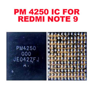
The PM4250 is a highly advanced Power Management Integrated Circuit (PMIC) designed by Qualcomm, specifically engineered to support the Snapdragon 662 and similar mid-tier 600-series processors. In modern smartphone architecture, it serves as the primary energy distributor, converting the raw battery voltage into multiple precise “rails” that power the CPU, RAM, and internal modems. PM 4250 Original Mobile Phone IC
Below is the comprehensive technical breakdown and specifications for the original PM4250 IC. PM 4250 Original Mobile Phone IC
PM4250 Technical Specifications Table
| Feature | Detailed Specification |
| Manufacturer | Qualcomm Technologies, Inc. |
| Part Number | PM-4250-0 (Commonly labeled PM4250 000) |
| Compatible SoCs | Snapdragon 662, 460, and select MTK Helio G85 variants |
| Package Type | WLCSP (Wafer Level Chip Scale Package) / QFN-144 |
| Input Voltage Range | 3.0V to 5.5V (Optimized for 4.4V Li-Po Batteries) |
| Step-Down (Buck) Converters | 4 to 6 Independent Phases (Efficiency >90%) |
| LDO Regulators | 15+ Low-Dropout Regulators (0.8V to 3.3V range) |
| Max Output Current | Up to 5A (High-current rails for CPU/GPU) |
| Control Interface | SPMI (System Power Management Interface) |
| Charging Support | Quick Charge 3.0+ / USB-PD 2.0 Negotiation |
| Operating Temperature | -40°C to +125°C (Extreme Thermal Resilience) |
| Safety Mechanisms | OVP, UVLO, Thermal Shutdown, PGOOD Signal |
1. Functional Overview and Architecture
The PM4250 is more than just a voltage regulator; it is a Power Management Unit (PMU). Its internal architecture is divided into specialized zones:
-
Switching Regulators (Bucks): These handle high-current tasks. For example, the VDD_CORE rail, which powers the processor cores, requires high amperage but very low voltage (around $1.1\text{V}$). The PM4250 uses Pulse Width Modulation (PWM) to provide this power with minimal heat loss. PM 4250 Original Mobile Phone IC
-
Linear Regulators (LDOs): These are used for “clean” power. Components like the Camera Sensor or Audio DAC are sensitive to electrical noise. The PM4250’s LDOs filter the power to ensure there is no “hiss” in the audio or “grain” in the photos. PM 4250 Original Mobile Phone IC
-
GPIO and Logic: The IC contains several General Purpose Input/Output pins that communicate with the phone’s power button and the SoC’s bootloader to initiate the startup sequence. PM 4250 Original Mobile Phone IC
2. Common Device Compatibility
The PM4250 is widely utilized in “best-seller” mid-range devices due to its balance of cost and efficiency. Notable devices include:
-
Xiaomi: Redmi 9T, Redmi Note 9 (Global), Poco M3.
-
Motorola: Moto G9, Moto G10, XT2083, XT2091.
-
Realme/Oppo: Various 600-series Snapdragon models.
3. Comparison with PM8940
While the PM8940 (which we discussed earlier) was the standard for the Snapdragon 435 era, the PM4250 represents a significant upgrade:
-
Efficiency: The PM4250 features higher switching frequencies, allowing for smaller external inductors and better battery life.
-
Thermal Headroom: It is rated for a higher operating temperature (up to 125°C) compared to older generations.
-
Charging Intelligence: It integrates more logic for USB-C Power Delivery (PD) negotiation, which was not as prevalent during the PM8940’s lifecycle.
4. Technician’s Repair Guide
In the repair industry, the PM4250 is known for thermal stress failure. Because it handles high current for fast charging (18W+), the solder balls underneath the chip can develop micro-cracks over time.
-
Symptom of Failure: The device shows a “vibration only” on startup, or the charging current stays stuck at $0.10\text{A}$ (indicating the IC hasn’t “handshaked” with the charger).
-
Reballing/Replacement: This is a 144-pin BGA/QFN. Technicians must use a dedicated PM4250 Stencil and high-quality leaded solder paste ($183^\circ\text{C}$ melting point) to ensure a reliable connection during rework.
More Products : https://gaffarmarketdelhi.com


