

358S1216 A2 Mobile Phone IC
Overview of the 358S1216 A2 Mobile Phone IC
The 358S1216 A2 Mobile Phone IC Mobile Phone Integrated Circuit (IC) is a cutting-edge component designed for modern mobile devices. Engineered for reliability and efficiency, this IC is perfect for ensuring seamless performance in handheld technology. 358S1216 A2 Mobile Phone IC
Top-Notch Compatibility & Performance
Whether you are repairing, assembling, or upgrading a mobile phone, the 358S1216 A2 IC offers universal compatibility with a range of devices. Its high-performance capabilities ensure faster processing times and efficient energy consumption, making it a critical addition to enhancing device longevity. 358S1216 A2 Mobile Phone IC
Why Choose the 358S1216 A2 IC?
Beyond basic functionality, this mobile phone IC stands out for its precision engineering and superior durability. It’s designed to meet the rigorous demands of today’s mobile technology, promising dependable and outstanding performance that you can trust. 358S1216 A2 Mobile Phone IC
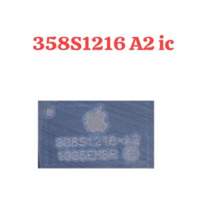
The 358S1216 A2 is a specialized Integrated Circuit (IC) primarily utilized in Apple mobile devices (iPhones and iPads) and some high-end Android smartphones. It functions as a Power Management Integrated Circuit (PMIC) with a specific focus on charging regulation and energy distribution. 358S1216 A2 Mobile Phone IC
Unlike general-purpose operational amplifiers like the LM358, the 358S1216 A2 is an Application-Specific Integrated Circuit (ASIC) designed to handle the complex power requirements of modern mobile motherboards. 358S1216 A2 Mobile Phone IC
Technical Specifications: 358S1216 A2
| Feature | Specification Details |
| IC Part Number | 358S1216 A2 |
| Category | Power Management IC (PMIC) / Charging IC |
| Commonly Used In | Apple iPhone series, iPad series, Xiaomi Mi A2 |
| Function | Battery Charging, Voltage Regulation, Power Distribution |
| Package Type | BGA (Ball Grid Array) |
| Pins/Balls | Varies by sub-revision (typically high-density micro-BGA) |
| Input Voltage (V_in) | 3.7V to 5.2V (Standard USB/Battery range) |
| Operating Temp | -25°C to +85°C |
| Primary Material | Silicon / Black Crystal Housing |
| Efficiency | High-efficiency switching regulator (>90% typical) |
Core Functions and Features
The 358S1216 A2 is not just a simple switch; it is the “brain” of the charging sub-system. Its responsibilities include:
1. Battery Management and Charging
The IC regulates the current flowing from the charging port to the lithium-ion battery. It supports multi-stage charging:
-
Constant Current (CC): Fast-charging the battery when it is low. 358S1216 A2 Mobile Phone IC
-
Constant Voltage (CV): Topping off the battery safely as it reaches 100%. 358S1216 A2 Mobile Phone IC
-
Trickle Charge: Maintaining the battery at very low currents to prevent degradation. 358S1216 A2 Mobile Phone IC
2. Thermal Protection
Mobile devices generate significant heat during fast charging. The 358S1216 A2 features internal thermal sensors. If the IC detects that the motherboard temperature is exceeding safe limits, it automatically throttles the charging current to prevent hardware damage or battery swelling. 358S1216 A2 Mobile Phone IC
3. Power Path Management
This IC enables the “Power Path” feature, allowing the device to run directly from the charger even if the battery is completely flat or disconnected. It intelligently splits the incoming power between the system load and the battery. 358S1216 A2 Mobile Phone IC
Application and Device Compatibility
The “A2” suffix denotes the revision of the silicon. This specific version is highly sought after by technicians for repairing power-related issues in specific flagship models. 358S1216 A2 Mobile Phone IC
-
iPhone/iPad Integration: It is often found near the battery connector on the logic board, managing the handshake between the Lightning/USB-C cable and the internal power rails.
-
Android Devices: Specifically used in the Xiaomi Mi A2 and certain ASUS Zenfone models where high-efficiency power conversion is required. 358S1216 A2 Mobile Phone IC
Troubleshooting and Common Failures
Because the 358S1216 A2 deals with high current and external power sources, it is a common point of failure. Typical symptoms of a faulty IC include:
-
Fake Charging: The phone shows a lightning bolt icon, but the battery percentage does not increase.
-
No Power: The device fails to turn on even with a known good battery.
-
Excessive Heat: The area near the IC becomes extremely hot immediately after plugging in a charger.
-
Dead on USB: The device is not recognized by a computer and draws 0.00A of current on a USB ammeter.
Note for Technicians: Replacing this IC requires professional micro-soldering tools. Since it is a BGA chip, it requires a hot air rework station, high-quality flux, and a specific reballing stencil.
Comparison: 358S1216 A2 vs. Standard Charging ICs
| Feature | 358S1216 A2 | Standard BQ-Series IC (e.g., BQ24157) |
| Complexity | High (Integrated PMIC functions) | Moderate (Dedicated Charger) |
| Control Interface | I2C / SMBus | I2C |
| Protection | Over-voltage, Over-current, Thermal | Standard Over-voltage |
| Repair Difficulty | High (BGA Reballing required) | Moderate (SMD) |
More Products : https://gaffarmarketdelhi.com


