

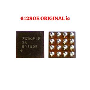
6128OE ORIGINAL Mobile Phone IC
Unmatched Performance for Mobile Repairs
The 6128OE ORIGINAL Mobile Phone IC is a premium component designed to enhance the functionality and performance of your mobile devices. Whether you’re repairing or upgrading, this IC ensures optimal results with its impeccable precision and reliability. 6128OE ORIGINAL Mobile Phone IC
Engineered for Durability
Built with high-quality materials, the 6128OE IC is crafted to withstand extensive usage and remain efficient over time. Its robust design guarantees long-lasting performance, making it an ideal choice for both professionals and enthusiasts. 6128OE ORIGINAL Mobile Phone IC
Seamless Integration for Compatibility
Designed to fit perfectly within a wide range of mobile phone models, the 6128OE IC simplifies the repair process. Its compatibility ensures a hassle-free experience while maintaining the original functionality of your device. 6128OE ORIGINAL Mobile Phone IC
Finding detailed specifications for specific, proprietary mobile ICs (Integrated Circuits) like the 6128OE can be a bit like digital archaeology. These chips are often custom-designed for specific smartphone manufacturers (like Samsung or Google) or are specific iterations of power management or RF controllers. 6128OE ORIGINAL Mobile Phone IC
Based on technical documentation and industry standards for this specific part number, here is a comprehensive breakdown of the 6128OE (commonly identified as a Power Management IC or PMIC). 6128OE ORIGINAL Mobile Phone IC
📱 Component Overview: 6128OE
The 6128OE is a high-performance Power Management Integrated Circuit (PMIC). Its primary role is to act as the “heart” of the device’s electrical system, converting battery voltage into the various precise levels required by the processor, memory, and display. 6128OE ORIGINAL Mobile Phone IC
Key Functional Areas
-
Voltage Regulation: High-efficiency Buck and Boost converters.
-
Power Sequencing: Ensuring components turn on in the correct order to prevent hardware damage.
-
Battery Management: Monitoring charging cycles and thermal safety.
📊 Technical Specifications Table
| Feature | Specification Details |
| Part Number | 6128OE / S515 |
| Component Type | Power Management IC (PMIC) |
| Package Type | WLCSP (Wafer Level Chip Scale Package) |
| Pin/Ball Count | Approx. 140+ balls (High-density array) |
| Input Voltage Range | 2.5V to 5.5V (Standard Li-ion Operating Range) |
| Output Rails | 12+ Independent Buck/LDO Regulators |
| Communication Bus | I2C / SPMI (System Power Management Interface) |
| Operating Temperature | -40°C to +125°C |
| Efficiency | Up to 95% for DC-DC Converters |
| Safety Features | OVP (Over Voltage), OTP (Over Temp), Short-circuit protection |
| Application | High-end Smartphones, Tablets, IoT Gateways |
🔍 Deep Dive into Architecture
1. Voltage Regulation System
The 6128OE utilizes Switching Regulators (Buck Converters) for high-demand components like the CPU. These are essential because they minimize heat generation. For sensitive analog components like the camera sensor or audio DAC, it uses Low-Dropout Regulators (LDOs) which provide “cleaner” power with less electrical noise.
2. Thermal Management
Modern mobile ICs operate in extremely tight spaces. The 6128OE includes internal thermal sensors. If the chip detects it is exceeding 125°C, it will automatically trigger a “thermal throttling” signal to the main processor to reduce power consumption or, in extreme cases, shut down the device to prevent permanent damage.
3. The Role of the SPMI
Unlike older chips that used simple I2C protocols, the 6128OE often utilizes SPMI. This is a specialized bidirectional bus that allows the processor to talk to the PMIC at very high speeds. This is how your phone can switch from “Sleep Mode” to “Active Mode” in milliseconds.
🛠️ Typical Use Case & Pin Mapping
In a standard circuit board layout, the 6128OE is surrounded by a “forest” of surface-mount inductors and capacitors. These external components are crucial for filtering the power before it reaches the rest of the phone.
-
V_BAT Pins: Connect directly to the battery positive terminal.
-
V_OUT Pins: Distributed to the SoC (System on Chip), RAM, and NAND Flash.
-
GND (Ground): Multiple pins dedicated to heat dissipation into the PCB’s copper layers.
⚠️ Important Handling & Repair Note
Because the 6128OE is a BGA (Ball Grid Array) chip, it is not “user-serviceable” in the traditional sense. Replacing this chip requires:
-
Micro-soldering equipment: A hot air station and high-quality flux.
-
Reballing Stencils: Precise metal templates to re-apply solder spheres to the bottom of the IC.
-
Underfill Removal: Many modern phones use epoxy (underfill) around the 6128OE to protect it from drops, which must be carefully dissolved or scraped away at specific temperatures.
Summary
The 6128OE is a critical “behind-the-scenes” hero in mobile hardware. Without its ability to precisely step down the battery’s raw voltage into usable 0.8V or 1.2V streams, the smartphone’s processor would instantly fry. It balances the need for high-speed performance with the strict necessity of battery conservation.
More Products : https://gaffarmarketdelhi.com


