

65132 BO ORIGINAL Mobile Phone IC
Reliable and High-Performance IC
The 65132 BO ORIGINAL Mobile Phone IC is designed to offer exceptional performance and durability for your mobile devices. Designed with precision, it ensures optimal functionality and supports smooth device operation. 65132 BO ORIGINAL Mobile Phone IC
Perfect Match for Top Brands
This integrated circuit is compatible with a wide range of mobile phone brands. Its robust design guarantees seamless integration to meet the technical needs of modern devices, ensuring longer device life and improved efficiency. 65132 BO ORIGINAL Mobile Phone IC
Quality You Can Trust
Manufactured to the highest standards, the 65132 BO ORIGINAL Mobile Phone IC provides reliable performance and enduring quality. Choose this product for unparalleled enhancement to your mobile devices, backed by advanced engineering and trusted manufacturing processes. 65132 BO ORIGINAL Mobile Phone IC
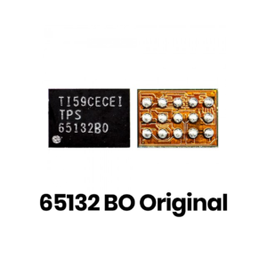
The 65132 B0 (often identified in full as the TPS65132B0) is a specialized Power Management Integrated Circuit (PMIC) widely used in modern smartphones and tablets. It is primarily responsible for providing the precise positive and negative voltage rails required to drive high-quality LCD displays. 65132 BO ORIGINAL Mobile Phone IC
Manufactured by Texas Instruments, this “Original” IC is critical for maintaining display clarity, touch responsiveness, and power efficiency in devices from brands like Oppo, Huawei, Vivo, and Xiaomi. 65132 BO ORIGINAL Mobile Phone IC
65132 B0 Technical Specifications
The following table outlines the core electrical and physical parameters of the 65132 B0 IC.
| Feature | Specification Detail |
| Manufacturer | Texas Instruments (TI) |
| Full Part Number | TPS65132B0YFFR |
| IC Function | Single Inductor – Dual Output (SIDO) Power Supply |
| Primary Application | LCD Display Bias (Smartphone/Tablet) |
| Input Voltage Range ($V_{IN}$) | $2.5\text{V}$ to $5.5\text{V}$ (Optimized for Li-Ion batteries) |
| Positive Output ($V_{POS}$) | $+4.0\text{V}$ to $+6.0\text{V}$ (Programmable in $0.1\text{V}$ steps) |
| Negative Output ($V_{NEG}$) | $-4.0\text{V}$ to $-6.0\text{V}$ (Programmable in $0.1\text{V}$ steps) |
| Max Output Current | $80\text{mA}$ to $150\text{mA}$ (Depending on configuration) |
| Efficiency | $>90\%$ at loads $>40\text{mA}$ |
| Switching Frequency | $1.6\text{MHz}$ |
| Control Interface | $I^2C$ Digital Interface |
| Package Type | $15\text{-Ball}$ DSBGA (Chip Scale Package) |
| Package Dimensions | $2.11\text{mm} \times 1.51\text{mm}$ |
Key Functional Features
The 65132 B0 is preferred by smartphone engineers because it solves the “dual rail” problem with extreme efficiency.
-
Single Inductor Design: Unlike older PMICs that required two separate inductors for positive and negative rails, this IC uses a single inductor to generate both. This saves significant board space—a premium in slim smartphones.
-
Programmable Sequencing: Through the $I^2C$ interface, manufacturers can program the exact power-up and power-down sequence to prevent “ghosting” or damage to the LCD panel.
-
Active Output Discharge: When the screen is turned off, the IC quickly discharges the voltage rails to ensure the display shuts down instantly without leaving a residual image.
-
Thermal Protection: Includes built-in thermal shutdown and under-voltage lock-out (UVLO) to prevent the IC from burning out during a short circuit.
Symptoms of a Faulty 65132 B0 IC
In mobile repair, this chip is a frequent culprit when the following issues occur:
-
No Display (Black Screen): The phone vibrates and makes sounds, but the screen remains black because the bias voltages ($+5\text{V}$/$-5\text{V}$) are missing.
-
Dim Screen or Flickering: If the IC fails to provide a stable $V_{POS}$, the backlight or liquid crystals may flicker.
-
Abnormal Battery Drain: A partial short inside the IC can cause the phone to consume excessive power even when the screen is off.
-
Overheating Near the Display Connector: Because this IC handles high-speed switching, a failure often results in localized heat on the motherboard.
Comparison: 65132 A0 vs. 65132 B0
Technicians often encounter different versions of this chip. While they are from the same family, their default factory settings differ:
| Feature | 65132 A0 (Oppo/Vivo) | 65132 B0 (Huawei/Global) |
| Default $V_{OUT}$ | Typically $\pm5.0\text{V}$ or $\pm5.4\text{V}$ | Variable based on OEM firmware |
| Output Current | Standard $80\text{mA}$ | Higher $150\text{mA}$ capable |
| Compatibility | Often interchangeable with software | Recommended for specific high-res panels |
Repair Recommendation
When replacing this IC, it is vital to use the Original version. “Copy” or “China Grade” ICs often lack the $1.6\text{MHz}$ switching stability, leading to “touch lag” or display noise (snowy lines) on the screen.
More Products : https://gaffarmarketdelhi.com


