

77916-11 Mobile Phone IC
Enhance Your Device’s Functionality
The 77916-11 Mobile Phone IC is an advanced and efficient integrated circuit, engineered to optimize the performance of your mobile devices. Whether it’s improving connectivity, extending battery life, or ensuring seamless operation, this component excels in delivering reliable results for modern smartphones. 77916-11 Mobile Phone IC
High-Quality Engineering for Modern Devices
Designed with precision, the 77916-11 Mobile Phone IC meets the demands of cutting-edge technology. Crafted for durability and efficiency, it supports your device’s internal systems while maintaining consistent, high-speed performance across applications. The IC is compatible with a wide range of mobile devices, ensuring unparalleled adaptability.
Perfect Choice for OEMs and Repairs
Whether you’re an OEM looking for dependable components or performing smartphone repairs, the 77916-11 Mobile Phone IC is the ideal choice. Its robust design ensures it meets industry standards and delivers sustainable performance. Trust in this innovative solution to keep your devices running smoothly. 77916-11 Mobile Phone IC
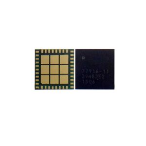
The SKY77916-11 (often referred to simply as the 77916-11) is a highly integrated Transmit / Receive Front-End Module (FEM) developed by Skyworks Solutions. It is part of the SkyLiTE™ family, specifically designed for 3G and 4G handsets. 77916-11 Mobile Phone IC
This IC acts as the “brawn” of the phone’s radio frequency (RF) system, amplifying signals so they can reach distant cell towers and switching between transmit and receive modes with high precision. 77916-11 Mobile Phone IC
Technical Specifications Table
| Feature | Specification Details |
| Manufacturer | Skyworks Solutions, Inc. |
| Part Number | SKY77916-11 (SkyLiTE™) |
| Function | Tx-Rx Front-End Module (FEM) / Power Amplifier (PA) |
| Supported Bands | Quad-Band GSM/GPRS/EDGE, Dual-Band TD-SCDMA, TDD LTE Band 39 |
| Technology | GaAs Heterojunction Bipolar Transistor (HBT) / CMOS |
| Input Impedance | 50 $\Omega$ (Internally matched) |
| Output Impedance | 50 $\Omega$ (Internally matched) |
| Control Interface | MIPI® RFFE (Radio Frequency Front End) |
| TRx Ports | 14 Linear Transmit/Receive Ports (5 Ultra-low loss) |
| Package Type | 38-pad MCM (Multi-Chip Module) |
| Dimensions | 5.5 mm x 5.3 mm x 0.8 mm (Max height) |
| Efficiency (GSM) | ~40% for GSM850/900; ~36% for DCS1800/PCS1900 |
| Input Power Range | –1 dBm to 6 dBm (GMSK modes) |
| Operating Temp | -30°C to +85°C (Standard industrial range) |
Key Features & Capabilities
1. Multi-Mode Support
The 77916-11 is designed to be a “one-stop shop” for cellular connectivity. It handles traditional 2G (GSM/EDGE) alongside 3G and 4G LTE signals. This makes it a staple in mid-range smartphones like the Xiaomi Redmi Note series and various Lenovo/Samsung models.
2. High Integration
The module integrates several critical components into a single tiny square:
-
Power Amplifiers (PA): Separate blocks for Low Band (LB) and High Band (HB).
-
Antenna Switch: A high-linearity switch that routes signals to the antenna.
-
Directional Coupler: Built-in broadband coupler for power monitoring, removing the need for external components.
-
ESD Protection: Built-in IEC-compliant protection to prevent damage from static discharge at the antenna.
3. Power Management & Efficiency
The IC utilizes Finger-Based Integrated Power Amplifier Control (FB-iPAQ). This technology minimizes output power variation even when the antenna match is poor (mismatch), ensuring the phone doesn’t drop calls or overheat when you hold it in a way that blocks the signal.
4. Coexistence Filters
It includes an integrated noise suppression notch filter specifically for WiFi coexistence. This prevents the cellular LTE signals from interfering with your phone’s WiFi or Bluetooth connection while both are active.
Application and Repair Notes
In the mobile repair industry, the 77916-11 is a “Network PA IC.” When this chip fails, the phone typically exhibits “No Service,” “Emergency Calls Only,” or very weak signal strength.
Note for Technicians: Because this is a BGA (Ball Grid Array) component with 38 pads on a multi-layer laminate substrate, replacement requires a hot air rework station and precision soldering. The IC is sensitive to moisture (MSL rating) and excessive heat during the “reballing” process.
PIN Configuration Summary
While the full pin-map is proprietary to the datasheet, the 38-pad layout generally follows this architecture:
-
VCC Pads: Main power supply for the GaAs HBT amplifiers.
-
MIPI Pads (SCLK, SDATA): For digital communication with the phone’s processor.
-
RF In/Out: Dedicated ports for different frequency bands (GSM, LTE B39, etc.).
-
GND: Large center pads for thermal dissipation and electrical grounding.
More Products : https://gaffarmarketdelhi.com
Official Website :


