

BQ 24261 M Original Mobile Phone IC
Enhance Your Mobile Devices with the BQ 24261 M IC
Looking for a dependable solution to improve the performance of your mobile devices? The BQ 24261 M Original Mobile Phone IC is designed to deliver optimal efficiency and seamless functionality. Crafted to meet high-quality standards, this IC is the ideal component for maintaining your device’s reliability. BQ 24261 M Original Mobile Phone IC
Why Choose the BQ 24261 M Original IC?
This mobile phone IC stands out due to its superior design and precision engineering. Whether you’re repairing or upgrading, its consistent performance ensures that your mobile device operates at its best. It’s a trusted choice for professionals in the repair industry and tech enthusiasts alike. BQ 24261 M Original Mobile Phone IC
Designed for Versatility and Efficiency
The BQ 24261 M IC is compatible with a wide range of mobile models, making it a versatile addition to your component inventory. Its original build guarantees durability and optimum energy management, ensuring that your devices stay powered and efficient for longer periods. BQ 24261 M Original Mobile Phone IC
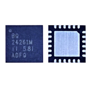
The BQ24261M is a highly integrated 3-A single-cell Li-ion battery charger and power path management IC. Widely used in smartphones like the Redmi Note 3 and various Infinix/Tecno models, it is known for its ability to handle high-current charging while maintaining a small footprint. BQ 24261 M Original Mobile Phone IC
Below is a detailed technical specification guide for the BQ24261M in English. BQ 24261 M Original Mobile Phone IC
1. Technical Specifications Table
| Parameter | Detailed Specification |
| Manufacturer | Texas Instruments (TI) |
| Device Type | Switch-mode Buck Charger with Power Path |
| Charging Current | Programmable up to 3.0 A |
| Input Voltage (VBUS) | 4.2 V to 10.5 V (Operating Range) |
| Max Input Voltage | 30 V (Absolute Maximum Rating) |
| Over-Voltage Protection | Integrated 10.5 V OVP |
| Efficiency | Up to 93% peak efficiency |
| OTG Output | 5.0 V @ 1.0 A (Boost Mode) |
| Switching Frequency | 1.5 MHz (High frequency for small inductors) |
| Interface | $I^2C$ Controlled (Host-mode) |
| Protection Features | JEITA Temperature monitoring, Thermal Shutdown, OVP, OCP |
| Package | 24-Pin VQFN (4.0 mm x 4.0 mm) |
2. Pin Configuration and Functions
The BQ24261M uses a 24-pin VQFN layout. Understanding these pins is crucial for mobile motherboard troubleshooting:
-
VBUS (Input): This pin receives power from the USB port or wall adapter. It is rated for 30V to protect against faulty chargers. BQ 24261 M Original Mobile Phone IC
-
SW (Switch): Connected to the external inductor. This is where the voltage is “stepped down” to charge the battery. BQ 24261 M Original Mobile Phone IC
-
SYS (System): This pin provides power to the phone’s internal circuits. The BQ24261M prioritizes this output so the phone can turn on even if the battery is dead. BQ 24261 M Original Mobile Phone IC
-
BAT (Battery): Connection point for the positive terminal of the Li-ion battery.
-
SDA/SCL ($I^2C$): The data and clock lines used by the CPU to tell the IC how fast to charge. BQ 24261 M Original Mobile Phone IC
-
STAT: An open-drain output that indicates the charge status (typically connected to a LED or a GPIO on the CPU).
3. Power Path Management (NVDC Architecture)
One of the “Original” features of the BQ24261M is the Narrow VDC (NVDC) power path. Traditional chargers connect the battery directly to the system. However, the BQ24261M places a MOSFET between the battery and the system.
Benefits of NVDC in Mobile Phones:
-
Instant-On: If your battery is at 0%, the phone will still boot up immediately when plugged in because the IC regulates the SYS pin voltage independently.
-
Battery Supplement Mode: If the phone’s CPU suddenly needs more power than the charger can provide (e.g., during a camera flash), the IC “borrows” power from the battery to assist the charger.
4. Charging Phases
The IC manages the battery life cycle through three distinct phases:
-
Pre-charge: If the battery voltage is below a certain threshold (usually $3.0\text{V}$), the IC applies a small current to “wake up” the cells safely.
-
Constant Current (CC): Once the battery is healthy, it pumps in the maximum current (up to $3\text{A}$) to charge the phone quickly.
-
Constant Voltage (CV): As the battery nears $4.2\text{V}$ or $4.4\text{V}$, the current is slowly reduced to ensure the battery reaches 100% capacity without overheating.
5. Mobile Repair & Troubleshooting Tips
In the mobile repair industry, the BQ24261M is often the culprit for specific power issues. Here is how to diagnose it:
-
VBUS Presence: If you plug in a charger and don’t see $5\text{V}$ at the VBUS pin, the charging port or the OVP MOSFET is likely broken.
-
No Charging (Fake Charging): If the phone shows a charging logo but the current draw (measured by a USB meter) is $0\text{mA}$ or very low, the BQ24261M may be “leaky” or the $I^2C$ communication with the CPU is failing.
-
Overheating: If the area around the inductor ($1\text{uH}$ coil) gets extremely hot, the IC is likely shorted internally.
-
OTG Failure: If the phone fails to read USB drives, the “Boost” part of this IC might be damaged, as it is responsible for outputting $5\text{V}$ to the USB port.
6. Conclusion
The BQ24261M is a robust, high-performance charging solution. Its high voltage tolerance ($30\text{V}$) makes it much more durable against cheap local chargers compared to older ICs. It balances fast charging speed with sophisticated safety protocols like JEITA, ensuring the mobile battery doesn’t degrade prematurely.
Official Website : https://gaffarmarketdelhi.com


