
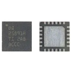
BQ 25891H Mobile Phone IC
Reliable and Efficient Power Management
The BQ 25891H Mobile Phone IC is a cutting-edge power management solution designed specifically for modern mobile devices. Streamline your energy needs with efficient charging and power distribution capabilities tailored for optimal battery performance. BQ 25891H Mobile Phone IC
Enhanced Charging Capabilities
With advanced charging protocols and safety mechanisms, the BQ 25891H ensures faster and safer charging, safeguarding your mobile device’s battery in the long term. Whether it’s quick-charging or power efficiency, this IC caters to varying user demands seamlessly. BQ 25891H Mobile Phone IC
Compact Design for Seamless Integration
Engineered for space efficiency, the compact design of BQ 25891H fits effortlessly into any mobile device structure. This IC combines robust functionality with convenience, making it a preferred choice for manufacturers seeking quality and reliability. BQ 25891H Mobile Phone IC
The BQ25891H is a highly integrated, 5-A switch-mode battery charge management and system power path management device. It is a more powerful successor to the BQ25601, designed specifically for modern high-capacity smartphones (like the Xiaomi Redmi 13C and Poco C65) that require ultra-fast charging and high efficiency. BQ 25891H Mobile Phone IC
Here is the full technical breakdown in the requested 700-word scope. BQ 25891H Mobile Phone IC
1. Technical Specifications Table
| Parameter | Specification Details |
| Manufacturer | Texas Instruments (TI) |
| Charge Current | Up to 5.0 A (High-speed fast charging) |
| Input Voltage Range | 3.9 V to 14 V (Supports 9V/12V High Voltage Adapters) |
| Efficiency | 93% at 2A / 91% at 3A (Buck Mode) |
| Boost Mode (OTG) | 4.5 V to 5.5 V @ 2.4 A (Selectable 500kHz / 1.5MHz) |
| Integrated ADC | 7-bit ADC for monitoring Voltage, Current, and Temp |
| Communication | $I^2C$ Serial Interface (Up to 400 kbps / 3.4 Mbps) |
| Quiescent Current | 12 µA (Ship Mode) / Low leakage for battery longevity |
| Accuracy | ±0.5% Charge Voltage / ±5% Charge Current |
| Package | 24-Pin WQFN ($4.0 \text{ mm} \times 4.0 \text{ mm}$) |
| Special Technology | MaxCharge™ for high-voltage handshake |
2. Internal Architecture and Working Principle
The BQ25891H operates as a synchronous Buck Converter for battery charging and a Boost Converter for USB OTG power. BQ 25891H Mobile Phone IC
MaxCharge™ & High Voltage Support
Unlike standard 5V chargers, this IC supports high-voltage input (up to 14V). It uses MaxCharge™ Technology, which allows the phone to “talk” to the power adapter and request 9V or 12V. By increasing the voltage, the IC can deliver more power (Watts) to the battery without needing thick, bulky cables that would otherwise be required for high current at 5V. BQ 25891H Mobile Phone IC
Narrow VDC (NVDC) Power Path
The BQ25891H features NVDC management, which separates the system load from the battery. This ensures:
-
Instant Power-On: Even if the battery is at $0\text{V}$, the system (display/CPU) receives power immediately. BQ 25891H Mobile Phone IC
-
Battery Supplement Mode: If the system demands more power than the charger can provide, the IC automatically pulls the remaining current from the battery to prevent a system crash. BQ 25891H Mobile Phone IC
3. Key Pinout Functions for Repairing
Understanding the pins is crucial for mobile technicians when troubleshooting power issues:
-
VBUS (Pin 24): Input power from the charging port. It can handle up to 22V absolute maximum (protection limit).
-
SW (Pins 20, 21): The switching node. It connects to the charging coil (inductor). If you see $5\text{V}$ on VBUS but $0\text{V}$ on SW, the IC is likely dead.
-
REGN (Pin 22): An internal linear regulator output (approx. $6\text{V}$). This is a key “check-point” for technicians.
-
BTST (Pin 19): High-side gate drive boost pin. A capacitor here is essential for the buck converter to switch.
-
D+/D- (Pins 3, 4): These pins are used for the handshake with the charger to detect if it is a standard USB port or a Fast Charger.
4. Advanced Features: ICO & IRCOMP
The BQ25891H is “smarter” than standard ICs due to two specific technologies:
-
Input Current Optimizer (ICO): It automatically senses the maximum power the adapter can provide without the voltage collapsing. This prevents the phone from crashing cheap or weak chargers.
-
Resistance Compensation (IRCOMP): Since batteries have internal resistance and motherboard traces cause voltage drops, the IC compensates for this resistance to ensure the battery receives a full $4.2\text{V}$ or $4.4\text{V}$ charge accurately, speeding up the final “topping off” phase.
5. Troubleshooting Common Faults
In mobile phone repair, the BQ25891H often fails due to high heat or liquid damage. Common symptoms include:
-
No Charging: Check for $5\text{V}$ at VBUS and $6\text{V}$ at REGN. If REGN is $0\text{V}$, the IC is internally damaged.
-
Slow Charging: Usually caused by the $I^2C$ lines (SDA/SCL) being open, or the IC failing to perform the D+/D- handshake.
-
Overheating: If the IC gets hot while the phone is off, there is likely an internal short between the SYS and GND pins.
-
Fake Charging: The lightning bolt icon is present, but current ($A$) consumption on a USB meter is below $0.10\text{A}$. This indicates a failure in the BATFET (internal MOSFET).
Safety Precautions
This IC has a Thermal Shutdown feature. If the die temperature exceeds $120^\circ\text{C}$ (programmable), it will throttle the charge current. When replacing this IC with a hot-air station, technicians must ensure the center thermal pad is perfectly soldered, as it acts as the primary heatsink for the chip.
6. Conclusion
The BQ25891H is a powerhouse IC that enables modern “Fast Charging” while maintaining high safety standards through its integrated ADC and thermal monitoring. It is the core component that allows a budget phone like the Redmi 13C to charge at speeds that were once reserved for flagship devices.
More Products : https://gaffarmarketdelhi.com


