DA9214 Mobile Phone IC
Highly Efficient Power Management
The DA9214 Mobile Phone IC is designed to ensure optimal power management in your mobile devices. With cutting-edge technology, it delivers precision and efficiency, enabling stable performance across various applications. DA9214 Mobile Phone IC
Compact and Versatile
This IC is compact in size, making it an excellent choice for devices where space is a premium. Its versatile design supports a broad range of mobile platforms, enhancing device compatibility and ease of integration. DA9214 Mobile Phone IC
Robust Performance
Engineered for reliability, the DA9214 offers robust performance that caters to the demands of modern mobile devices. Whether you’re optimizing battery life or ensuring smooth operation, this intelligent solution has got you covered. DA9214 Mobile Phone IC
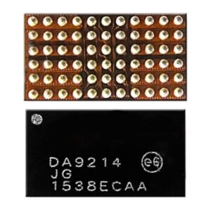
The DA9214 (manufactured by Renesas, formerly Dialog Semiconductor) is a high-performance, synchronous multiphase DC-DC buck converter designed primarily as a sub-Power Management IC (sub-PMIC). It is engineered to supply the high-current demands of modern smartphone processor cores (CPUs), Graphics Processing Units (GPUs), and DDR memory. DA9214 Mobile Phone IC
The following tables and sections provide a comprehensive breakdown of its technical specifications and functional capabilities.
1. Primary Technical Specifications
The DA9214 is distinguished by its ability to deliver high current (up to 20A total) with exceptional efficiency and a very small footprint. DA9214 Mobile Phone IC
| Feature | Specification |
| Manufacturer | Renesas Electronics (formerly Dialog Semiconductor) |
| IC Type | Multiphase Synchronous Buck Converter (Sub-PMIC) |
| Input Voltage Range | 2.8 V to 5.5 V (Compatible with 1S Li-Ion batteries) |
| Output Voltage Range | 0.3 V to 1.57 V (Programmable) |
| Max Output Current | 20 A Total (2 x 10 A channels) |
| Switching Frequency | 3 MHz (Nominal) |
| Efficiency | >90% (Optimized for high-load scenarios) |
| Communication Interface | I2C and SPI compatible |
| Operating Temperature | -40°C to +85°C (Standard) / up to +105°C (Automotive) |
| Package Type | 66-ball WL-CSP (0.4mm pitch) or 66-ball VFBGA (0.5mm) |
2. Detailed Performance & Electrical Characteristics
The DA9214 utilizes a multiphase topology to distribute heat and reduce the size of external components, specifically the inductors. DA9214 Mobile Phone IC
| Parameter | Value / Detail |
| Number of Phases | 4 Phases (configured as 2 + 2 for dual output) |
| Voltage Accuracy | ±1% (Static) / ±3% (Dynamic) |
| Load Transient Response | 10 A/µs (Supports rapid processor state changes) |
| Inductor Profile | Supports low-profile inductors (<1 mm height) |
| Phase Shedding | Automatic (Improves efficiency at light loads) |
| Remote Sensing | Included (Sensing at the point of load for precision) |
| Soft Start | Programmable (Adjustable slope to prevent inrush current) |
| Protection Features | Over-temperature (OTP), Over-current (OCP), UVLO |
3. Pin Configuration & Hardware Interface
The IC is designed for complex mobile logic boards where space is at a premium. DA9214 Mobile Phone IC
-
Communication: Dual interface support allows it to be controlled by the main application processor via I2C for voltage scaling or SPI for faster telemetry.
-
GPIOs: Typically includes 3-5 General Purpose I/O pins that can be configured for Power Good signals, hardware-enable pins, or DVS (Dynamic Voltage Scaling) triggers.
-
DVS Support: Features dedicated DVS control to adjust output voltage on the fly, matching the CPU/GPU clock frequency to save power.
4. Key Features & Benefits
-
High Current Density: Delivering 20A from a package smaller than 12mm² is critical for high-end chipsets like the ARM Cortex-A15/A57 families.
-
Integrated Power Switches: Eliminates the need for external MOSFETs or Schottky diodes, significantly reducing the Bill of Materials (BOM) count.
-
Low Ripple: The 3 MHz switching frequency and multiphase interleaving minimize output voltage ripple, ensuring stable operation for sensitive 7nm/5nm processors.
-
Adaptive Power: Through “Phase Shedding,” the IC can shut down unused phases during sleep modes to conserve battery life.
5. Applications in Mobile Devices
The DA9214 is rarely the only PMIC in a phone; it acts as a “companion” or “sub-PMIC” specifically for the heaviest loads:
-
Smartphone Core Power: Powering the primary clusters of high-end SoCs (System on Chips).
-
GPU Power: Providing the high-burst current needed for intensive mobile gaming or 4K video rendering.
-
Tablets & Ultrabooks: Used in larger portable devices where high-wattage ARM or x86 mobile processors are used.
-
FPGA Powering: Suitable for high-speed field-programmable gate arrays in mobile infrastructure.
6. Physical Dimensions & Packaging
To fit inside thin modern devices, the DA9214 utilizes advanced wafer-level packaging.
| Package Option | Dimensions | Pitch |
| WL-CSP-66 | ~2.5 x 4.5 mm | 0.4 mm |
| VFBGA-66 | ~3.8 x 5.8 mm | 0.5 mm |
Note for Technicians: When replacing this IC during mobile repair, ensure the correct suffix is matched (e.g., DA9214-A for automotive or DA9214-XX for specific firmware/voltage variants), as the OTP (One-Time Programmable) memory settings for default start-up voltages may differ between models.
More Products : https://gaffarmarketdelhi.com