
HI 6555 V110 Mobile Phone IC
HI 6555 V110 Mobile Phone ICUncompromising Reliability for Mobile Devices
The HI 6555 V110 Mobile Phone IC is a state-of-the-art integrated circuit designed to meet the demanding performance requirements of modern mobile devices. Engineered for efficiency and durability, this IC offers seamless compatibility with a variety of smartphone architectures, ensuring dependable functionality that supports smooth device operation. HI 6555 V110 Mobile Phone IC
Advanced Features for Optimized Device Performance
What sets the HI 6555 V110 apart is its advanced design, which incorporates innovative technologies for power management and signal processing. Whether it’s enhancing battery efficiency or ensuring fast and reliable communication between device components, this IC does it all. The product’s streamlined design minimizes energy consumption without compromising performance, making it ideal for high-demand mobile applications. HI 6555 V110 Mobile Phone IC
Why Choose the HI 6555 V110 Mobile Phone IC?
For manufacturers and tech enthusiasts seeking impeccable quality and a cost-effective solution, the HI 6555 V110 is the perfect choice. Its compact form factor allows for easy integration into modern smartphones and other mobile devices, while its robust build ensures long-term reliability. Designed with precision, the IC delivers consistent performance, making it an excellent choice for professionals looking to optimize their electronic devices.
Upgrade your mobile engineering projects with the HI 6555 V110 Mobile Phone IC and experience superior performance, reliability, and efficiency tailored toward today’s tech-savvy consumer needs. HI 6555 V110 Mobile Phone IC
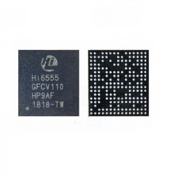
The HI6555 V110 is a specialized Power Management Integrated Circuit (PMIC) developed by HiSilicon, the semiconductor subsidiary of Huawei. This IC is a critical component in the power architecture of Kirin-based mobile platforms, primarily used in mid-range Huawei and Honor smartphones such as the Honor 6X, 7X, and GR5 Mini.
Below is the detailed technical specification and functional overview of the HI6555 V110.
Technical Specifications
| Feature | Details |
| Model Number | HI6555 V110 (GFCV110) |
| Manufacturer | HiSilicon (Huawei) |
| Function | Power Management IC (PMIC) / Connectivity Support |
| Package Type | Ball Grid Array (BGA) |
| Input Voltage Range | $3.4\text{V}$ to $4.4\text{V}$ (Typical battery voltage) |
| Output Rails | Multiple regulated outputs (LDOs and Buck converters) |
| Primary Voltage Outputs | $1.8\text{V}$, $1.2\text{V}$, $2.8\text{V}$ (Core/Peripheral supply) |
| Power Dissipation | Approximately $0.5\text{W}$ (depending on load) |
| Operating Temperature | $-25\text{°C}$ to $+85\text{°C}$ (Industrial Grade) |
| Compatibility | Kirin 650, Kirin 655, Kirin 658 Platforms |
| Main Applications | Power regulation, Audio processing, Connectivity control |
Key Functional Roles
The HI6555 V110 serves as the “heart” of the device’s electrical system. Its primary responsibilities include:
-
Voltage Regulation: It converts the raw battery voltage into multiple stable levels (Buck/Boost and LDO) required by the processor (CPU/GPU), memory (RAM), and display.
-
Audio Subsystem: In many Kirin architectures, this IC integrates audio codec functions, managing the digital-to-analog conversion for speakers and microphones.
-
Connectivity Support: It assists in managing the power states for Wi-Fi, Bluetooth, and GPS modules to ensure energy efficiency during standby modes.
-
Battery Management: It monitors thermal levels and charging sequences to prevent over-voltage or overheating during fast charging.
Common Signs of Failure
Because this IC manages the primary power rails, a faulty HI6555 V110 often results in:
-
Dead Device: The phone fails to trigger the boot sequence.
-
Charging Issues: The device shows a charging logo but doesn’t increase percentage, or doesn’t detect the charger at all.
-
Short Circuits: High heat dissipation near the PMIC area on the PCB (Motherboard).
-
Audio Failure: Loss of sound in both the earpiece and loud speaker despite software resets.
Repair & Installation Note
This is a BGA-type chip, meaning it is soldered using tiny lead or lead-free solder balls underneath the package. Replacing it requires professional tools, including a hot air rework station, high-quality flux, and often a reballing stencil if the IC is being reused. HI 6555 V110 Mobile Phone IC
More Products : https://gaffarmarketdelhi.com


