

PM 6150A Mobile Phone IC
High-Quality PM 6150A Mobile Phone IC
The PM 6150A Mobile Phone IC is designed to offer outstanding performance for modern mobile phone systems. Engineered with precision, this integrated circuit ensures seamless functionality and reliable power management, essential for optimal device performance. PM 6150A Mobile Phone IC
Reliable and Efficient Power Management
Created to support advanced connectivity and efficiency, the PM 6150A handles multiple operations expertly while minimizing energy consumption. Ideal for manufacturers and repair professionals, this IC guarantees durability and consistent performance under varied conditions. PM 6150A Mobile Phone IC
Compatible and Versatile Component
With broad compatibility across a range of mobile devices, the PM 6150A serves as a versatile solution for mobile phone enhancements and repairs. Whether for replacements or new assemblies, this IC is an indispensable addition to your toolkit. PM 6150A Mobile Phone IC
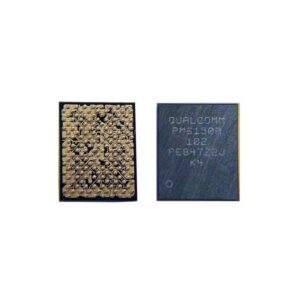
The PM6150A (typically the PM6150A-102 variant) is a high-performance Power Management Integrated Circuit (PMIC) designed by Qualcomm. It is a cornerstone of modern mid-to-high-tier smartphone hardware, particularly those utilizing Snapdragon 600 and 700 series chipsets. PM 6150A Mobile Phone IC
Unlike standard power ICs that handle simple regulation, the PM6150A acts as a Companion PMIC. It works alongside a primary PMIC (like the PM6150) to manage specific high-drain or precision rails such as the CPU/GPU core, memory interfaces, and camera sensors. PM 6150A Mobile Phone IC
PM6150A Technical Specifications
The following table outlines the core technical parameters and functional characteristics of the PM6150A.
| Feature/Parameter | Specifications |
| Manufacturer | Qualcomm |
| Part Number/Marking | PM6150A / PM6150A-102 |
| Type | Companion Power Management IC (PMIC) |
| Common Application | Smartphones, Tablets, IoT Devices |
| Pin Count | 40 Pins (Commonly found in SOT-23 or BGA variants) |
| Input Voltage Range | 3.6V – 4.5V (Standard Li-ion battery range) |
| Output Voltage | Configurable (Typically 0.6V to 3.3V) |
| Integrated Components | Buck Converters, LDO Regulators, Power Sequencers |
| Communication Bus | I²C / SPMI (System Power Management Interface) |
| Thermal Protection | Internal Thermal Shutdown & Overcurrent Latch |
| Packaging | BGA (Ball Grid Array) for mobile, QFP for industrial |
Key Functional Roles
The PM6150A is specialized for “heavy lifting” in the power architecture. Its primary roles include:
-
Processor Voltage Scaling: It provides the VDD_CORE and VDD_MIF rails. These are dynamic voltages that change based on whether your phone is idling or running a heavy game.
-
Camera & Display Support: It often manages the high-precision power required for image sensors and display driver logic (VCC_LCD).
-
Energy Efficiency: By offloading specific rails from the main PMIC, it reduces localized heat on the motherboard and improves battery longevity through efficient DC-DC conversion.
Compatibility and Deployment
The PM6150A is a versatile chip found across various brands due to its integration with Qualcomm reference designs.
Supported Platforms
It is most commonly found in devices using the following platforms:
-
Qualcomm Snapdragon 675 / 710 / 712 / 730G
-
Samsung Galaxy A Series (e.g., A70, A60)
-
Xiaomi Redmi Note Series (e.g., Note 7 Pro)
-
Vivo & Oppo Mid-tier models
Troubleshooting & Failure Symptoms
Because it sits at the heart of the power distribution, a faulty PM6150A usually results in a “Dead Board” scenario. Common symptoms include:
-
Zero Boot: The phone does not respond to the power button.
-
Short Circuit: The motherboard shows a high current draw on a DC Power Supply immediately upon connection.
-
Hanging on Logo: If the rails for memory or the GPU are unstable, the device may freeze during the boot sequence.
Maintenance & Repair Notes
Note: Replacing this IC requires professional micro-soldering skills. The PM6150A is a BGA chip, meaning it has tiny solder balls underneath that must be perfectly aligned with the motherboard pads.
-
Reballing: Use a 0.12mm stencil for the best results when re-applying solder balls.
-
Heat Sensitivity: Use a rework station set between 330°C and 350°C with medium airflow to avoid damaging the internal silicon die or surrounding components.
More Products ; https://gaffarmarketdelhi.com


