

PM 8250 Mobile Phone IC
Cutting-Edge Performance for Modern Devices
The PM 8250 Mobile Phone IC is crafted to meet the rigorous demands of today’s smartphones and mobile devices. Designed with top-tier engineering, it ensures optimal power distribution and enhances device performance for seamless connectivity and longer battery life. PM 8250 Mobile Phone IC
Reliable Power Management Solution
This integrated circuit excels at managing power flow, reducing energy waste, and supporting efficient device operation. Its compact design makes it an ideal choice for manufacturers seeking reliability and high efficiency in their devices. PM 8250 Mobile Phone IC
Compatibility and Versatility
The PM 8250 IC is versatile and compatible with a wide range of mobile devices, ensuring smooth integration and enhanced performance. Unlock the potential of your designs with this cutting-edge solution. PM 8250 Mobile Phone IC
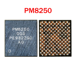
The PM8250 is a high-performance primary Power Management Integrated Circuit (PMIC) developed by Qualcomm. It is a flagship-grade chip designed specifically to complement the Snapdragon 865 chipset (SM8250). In the world of mobile repair and hardware engineering, the PM8250 is known for its extreme efficiency and high-density power delivery, powering iconic flagship devices like the Samsung Galaxy S20 series, Xiaomi Mi 10, and OnePlus 8. PM 8250 Mobile Phone IC
PM8250 Technical Specifications Table
| Feature Category | Technical Specification Detail |
| Manufacturer | Qualcomm |
| IC Model | PM8250 (Often paired with PM8150L and PM8150B) |
| Architecture | Mixed-Signal Power Management System |
| Package Type | 161-pin FOWPSP (Fan-Out Wafer-Level Pico-Scale Package) |
| Dimensions | $4.49 \times 5.07 \times 0.55\text{ mm}$ |
| Voltage Input (VBAT) | $3.4\text{V}$ to $4.8\text{V}$ |
| SMPS Channels | 10 Buck Converters (2x HFS510, 8x FTS510) |
| LDO Regulators | 18+ Low Dropout Linear Regulators |
| Interface | Dual-line SPMI (System Power Management Interface) |
| Crystal Support | $38.4\text{ MHz}$ XO (External Oscillator) Controller |
| GPIOs | 10 Configurable General Purpose I/Os |
| Protection | Thermal, Over-Current (OCP), Under-Voltage (UVLO) |
| ADC | Integrated on-chip HK/XO ADC for Housekeeping |
Core Functionality and Power Rails
The PM8250 is the “Primary” controller, meaning it is responsible for the most critical boot sequences and power grids. Unlike mid-range ICs, it uses a sophisticated Sub-regulation system. Instead of dropping high battery voltage directly to low-voltage LDOs, it creates intermediate rails (around $1.3\text{V}$) via high-efficiency Buck converters, which then feed the LDOs. This significantly reduces heat and extends battery life.
1. Switching Regulators (Bucks)
The 10 Buck converters are the “heavy lifters”:
-
HFS510 (High Frequency): These are designed for ultra-fast transient responses, feeding the most demanding parts of the Snapdragon CPU.
-
FTS510 (Fast Transient): These manage the GPU and Modem rails, ensuring that when you start a heavy game, the power delivery doesn’t sag, which would cause the phone to crash.
2. Clock Management
One of the most vital roles of the PM8250 is serving as the Clock Hub. It manages the $38.4\text{ MHz}$ reference clock for the entire chipset. It also generates the Sleep Clock ($32.768\text{ kHz}$), which keeps the phone’s background tasks (like alarms and notifications) running while the screen is off.
Hardware Repair & Diagnostic Insights
For hardware technicians, the PM8250 is a critical point of failure in “Dead Boot” scenarios.
-
VPH_PWR Rail: The IC manages the main system voltage. If a multimeter shows a short on the capacitors surrounding the PM8250, the phone will typically show $0.00\text{A}$ or a very low, fluctuating current on a DC Power Supply.
-
OTP (One-Time Programmable) Memory: The PM8250 contains an internal OTP memory that stores the specific power-on sequence for the SM8250 CPU. This is why you cannot swap a PM8250 with a PM8150, even if they look identical; the boot “instructions” inside are different.
-
Thermal Protection: If the IC detects a temperature above $125^\circ\text{C}$, it triggers a Hard Reset. In many cases, if a phone is stuck in a “thermal restart” loop, the internal thermistor of the PM8250 might be faulty.
Difference Between PM8250 and PM8150L/B
In flagship 5G designs, the workload is split:
-
PM8250: Focuses on the “Core”—the Brain (CPU) and System logic. PM 8250 Mobile Phone IC
-
PM8150L: Often handles the “Lights”—Display backlight, Flash, and Vibrator. PM 8250 Mobile Phone IC
-
PM8150B: Focuses on the “Battery”—Charging logic and Fuel Gauge. PM 8250 Mobile Phone IC
Installation Precautions
Due to the 161-pin FOWPSP package, the balls are extremely small and close together (fine pitch).
-
Pre-Baking: Since these chips can absorb moisture, technicians often bake them at $100^\circ\text{C}$ for 24 hours before soldering to prevent the “popcorn effect” (internal cracking). PM 8250 Mobile Phone IC
-
Alignment: Any slight misalignment during reballing will lead to a bridge between VDD and Ground, instantly killing the IC upon power-up. PM 8250 Mobile Phone IC
More Products https://gaffarmarketdelhi.com


