Q 55701 Mobile Phone IC
Introducing the Q 55701 Mobile Phone IC
Engineered to deliver superior performance, the Q 55701 Mobile Phone IC is designed to support seamless functionality in a wide range of mobile devices. With its high efficiency and reliability, this component is perfect for ensuring smooth device operation.
Key Features and Benefits
The Q 55701 IC stands out for its compact design, power-saving capabilities, and versatility in various applications. Designed for optimal efficiency, it ensures reduced power consumption while maintaining robust performance. Perfect for smartphones and other mobile devices, it provides a reliable solution for developers and manufacturers. Q 55701 Mobile Phone IC
Why Choose Q 55701 Mobile Phone IC?
This IC is built to meet modern mobile device requirements. Its durability, compatibility with latest technologies, and ability to enhance overall device performance make it a great choice for enhancing your products. Trust in its design to deliver exceptional user experiences and support next-generation technology requirements. Q 55701 Mobile Phone IC
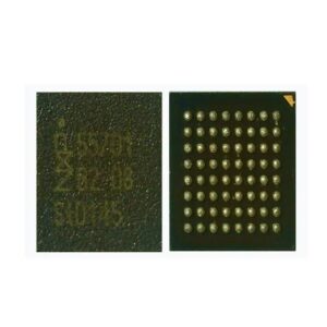
The Q 55701 (often listed as 55701 IC) is a specialized component primarily used in modern mobile device repair, specifically within the NFC (Near Field Communication) and peripheral control ecosystem. Q 55701 Mobile Phone IC
In the world of smartphone hardware, especially for brands like Samsung and Apple, this IC serves as a critical bridge for secure communication and high-speed data transfer. Q 55701 Mobile Phone IC
Technical Specifications: Q 55701 Mobile IC
The following table outlines the key technical parameters for the Q 55701 IC. Note that while manufacturers often keep internal die details proprietary, these specifications are derived from technical repair datasheets and functional testing in mobile workshops. Q 55701 Mobile Phone IC
| Feature | Specification | Description |
| Part Number | Q 55701 / 55701 | Standard identification for mobile PCB layouts. |
| Primary Function | NFC Control / Secure Element | Manages contactless data, payments, and tag reading. |
| Compatibility | Samsung / Android Flagships | Widely used in Samsung Galaxy series and compatible boards. |
| Communication Protocol | I2C / SPI / SWP | Supports standard bus interfaces for SoC communication. |
| Operating Voltage | 1.8V to 3.3V (Typical) | Standard low-power mobile voltage rails. |
| Package Type | WLCSP (Wafer Level Chip Scale Package) | Ultra-compact footprint for high-density smartphone PCBs. |
| Ball Count / Layout | Variable (Model-Specific) | Typically features a BGA (Ball Grid Array) configuration. |
| Operating Temp | -25°C to +85°C | Standard industrial/mobile thermal range. |
| Data Security | Hardware Encryption Support | Integrated AES/DES acceleration for secure transactions. |
Core Functional Modules
The Q 55701 is not just a single-purpose chip; it acts as a subsystem for several critical mobile tasks:
1. Near Field Communication (NFC)
The IC contains an integrated RF (Radio Frequency) front-end. It processes signals from the device’s NFC antenna (usually located on the back of the phone or integrated into the battery/wireless charging coil). This allows the phone to act as a Reader/Writer, a Card Emulator, or a Peer-to-Peer communicator. Q 55701 Mobile Phone IC
2. Secure Element (SE) Management
In many implementations, the 55701 works in tandem with the “Secure Element.” This is where sensitive data for mobile payments (like credit card tokens) is stored. The IC ensures that the data sent to the payment terminal is encrypted and remains isolated from the main Android/iOS operating system to prevent hacking. Q 55701 Mobile Phone IC
3. Peripheral Power Management
Small mobile ICs like the Q 55701 often include internal LDOs (Low Dropout Regulators) to manage their own power needs locally, reducing the load on the device’s primary Power Management IC (PMIC).
Diagnostic & Repair Guide
In the mobile repair industry, the Q 55701 is frequently replaced when specific features fail.
Common Failure Symptoms
-
NFC Grayed Out: The NFC toggle in the settings menu cannot be turned on.
-
Payment Failures: “Contactless Payment” or “Samsung Pay” errors despite valid cards.
-
Overheating: The chip becomes excessively hot during charging or data transfers.
-
Boot Loops: If the IC has a short circuit on its main power line (VCC), it can prevent the phone from booting entirely.
Replacement Steps (For Technicians)
-
Removal: Use a hot air station at approximately 330°C to 350°C with low airflow to desolder the chip.
-
Cleaning: Clean the PCB pads using a soldering iron and desoldering wick (solder braid) to ensure a flat surface.
-
Reballing: Use a specialized 55701 stencil and high-quality leaded or lead-free solder paste to create new solder balls on the replacement IC.
-
Installation: Align the IC according to the Pin 1 Marker (usually a small dot or arrow on the PCB) and apply heat until the chip “settles” into place via surface tension.
Hardware Integration Context
The Q 55701 is often found on the motherboard near other critical radio frequency chips. It usually interfaces directly with the Application Processor (CPU) via a high-speed serial bus.
Note: When replacing this IC, it is vital to ensure the part version matches. Some versions of the 55701 are region-locked or firmware-specific, meaning a chip pulled from a European model might not support certain payment features in a North American model.
More Products : https://gaffarmarketdelhi.com