
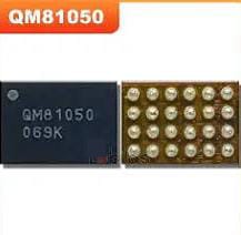
QM 81050 Mobile Phone IC
Advanced Technology for Optimal Performance
The QM 81050 Mobile Phone IC is engineered to enhance the functionality of your mobile devices with unparalleled efficiency and reliability. Designed with cutting-edge technology, this integrated circuit ensures seamless performance, optimizing the overall user experience. QM 81050 Mobile Phone IC
Compact and Durable Design
Compact yet robust, the QM 81050 is crafted for durability and space-saving integration within your device. Its innovative design improves energy efficiency, ensuring minimal power consumption without compromising on performance. QM 81050 Mobile Phone IC
Versatile Applications
The QM 81050 Mobile Phone IC is compatible with a wide range of mobile devices, making it the ideal solution for manufacturers seeking enhanced operational throughput. Elevate the capabilities of your devices with this high-performance integrated circuit.
The QM81050 is a specialized power management and RF support integrated circuit (IC) manufactured by Qorvo. It primarily functions as a high-efficiency Boost-Buck DC-DC Converter designed specifically for mobile devices, particularly to supply power to RF Power Amplifiers (PAs) in 4G and 5G systems. QM 81050 Mobile Phone IC
In many modern repair contexts, it is also referred to as a “Charging IC” or “Wireless Charging Support IC” because of its role in managing power rails for high-power subsystems like the BCM4389 WiFi/Bluetooth modules or wireless charging arrays. QM 81050 Mobile Phone IC
Technical Specifications Table
The following table outlines the core electrical and mechanical parameters for the QM81050 IC based on its official technical datasheet.
| Parameter Category | Specification Details | Value / Range |
| Manufacturer | Qorvo | — |
| Function | Boost-Buck DC-DC Converter | Power Management (PMU) |
| Supply Voltage ($V_{BAT}$) | Battery Supply Input | 2.5V to 5.1V |
| Output Voltage ($V_{CC}$) | Programmable Output Range | 0.0V to 5.5V |
| Output Current (Buck) | Max load in Buck mode ($V_{CC} < 3.4V$) | 1.0 A |
| Output Current (Boost) | Max load in Boost mode ($V_{CC} \geq 3.4V$) | 1.4 A |
| Efficiency (Buck) | Peak efficiency at typical load | ~93.0% |
| Efficiency (Boost) | Peak efficiency at typical load | ~86.5% |
| Switching Frequency | Internal Oscillator Range | 0.125 MHz to 7.875 MHz |
| Interface | Control Protocol | MIPI® RFFE (Programmable) |
| Voltage Resolution | DAC Step Resolution ($LSB$) | 50 mV |
| Transition Time | $1.0V$ to $5.5V$ Transition | < 10 µs |
| Startup Time | Initial Power-on Delay | < 20 µs |
| Protection Features | Built-in Safety | UVLO, OVP, OCP, OTP |
| Operating Temp | Extended Operational Range | -30°C to +85°C |
| Package Type | Footprint | WLCSP-24 or BGA-24 |
Detailed Functional Overview
1. Boost-Buck Architecture
The standout feature of the QM81050 is its ability to both “step up” (boost) and “step down” (buck) voltage. In a mobile phone, battery voltage fluctuates (typically between 3.2V and 4.2V). However, 5G Power Amplifiers often require stable voltages higher than what the battery can provide to maintain signal linearity and output power. QM 81050 Mobile Phone IC
-
Buck Mode: Saves energy when the required output is lower than the battery voltage. QM 81050 Mobile Phone IC
-
Boost Mode: Ensures the RF signal doesn’t “clip” or lose strength when the battery is low or when high power (HPUE) is required. QM 81050 Mobile Phone IC
2. MIPI® RFFE Control
Unlike simple regulators, the QM81050 is “intelligent.” It communicates with the phone’s baseband processor via the MIPI Radio Frequency Front End (RFFE) interface. This allows the processor to adjust the voltage in real-time (within microseconds) based on the signal strength required.
3. Application in Mobile Repair
While its datasheet labels it a DC-DC converter, in the repair industry, you will find this IC in the following subsystems:
-
RF Front End: Supplying the “VCC” rail to 4G/5G Power Amplifiers.
-
WiFi/Bluetooth Power: It is frequently found alongside Broadcom (BCM) modules in flagship devices like the Samsung Galaxy S-series and iPhones.
-
Wireless Charging: It acts as a secondary regulator for wireless charging power paths to ensure stable 5V delivery to the battery management system.
Pin Configuration and Integration
The IC usually comes in a WLCSP-24 (Wafer Level Chip Scale Package) with 24 solder balls.
Typical Pin Assignments:
-
VBATT1 / VBATT2: Main battery inputs.
-
VIO: Supply for the MIPI digital interface.
-
SCLK / SDATA: MIPI RFFE clock and data lines.
-
Lbuck: Connection point for the external power inductor (critical for the conversion process).
-
Vout_fb: Feedback loop to ensure the output voltage remains accurate.
-
GND / GNDA: Grounding pins (analog and digital).
Note for Technicians: When replacing this IC, proper grounding is vital. The chip generates significant heat during high-power boost operations. Ensure the PCB ground plane is solid and the solder balls are perfectly aligned to prevent “thermal runaway” or signal oscillation.
Comparison with Similar ICs
| Feature | QM81050 | Standard Buck Converter |
| Direction | Dual (Boost & Buck) | Single (Buck only) |
| Speed | Ultra-Fast (<10µs) | Slow (>100µs) |
| Control | MIPI RFFE | PWM / Analog |
| Use Case | 5G RF / Flagship WiFi | General Power Rails |
More Products : https://gaffarmarketdelhi.com


