
QPA8685 Mobile Phone IC
High-Performance IC for Advanced Mobile Devices
The QPA8685 Mobile Phone IC is a cutting-edge component designed to meet the ever-growing demands of modern smartphones. Engineered to deliver efficient performance, this IC ensures seamless functionality and enhances the overall user experience of your mobile devices.
Reliable and Energy-Efficient Design
The QPA8685 sets itself apart with its reliability and energy-efficient operation. It optimizes power consumption while maintaining exceptional performance, making it an ideal choice for manufacturers looking to build smartphones that last longer on a single charge. QPA8685 Mobile Phone IC
Compact and Versatile Solution
Designed for versatility, the QPA8685 is compact yet highly capable, making it suitable for various smartphone designs. Its advanced features help reduce device size without compromising on performance, giving you the flexibility to innovate without limitations. QPA8685 Mobile Phone IC
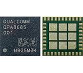
The QPA8685 is a high-performance Radio Frequency (RF) Front-End (RFFE) Power Amplifier (PA) Module developed by Qualcomm. It is a critical component in the wireless communication architecture of modern smartphones and wearable devices, particularly those utilizing the Snapdragon Wear and mid-range mobile platforms. QPA8685 Mobile Phone IC
Its primary role is to amplify weak RF signals before they are sent to the antenna, ensuring stable cellular connectivity across various network bands including 2G, 3G, and 4G LTE. QPA8685 Mobile Phone IC
1. Technical Specifications Table
The following table summarizes the core technical parameters of the QPA8685 IC based on its integration within the Qualcomm RFFE ecosystem.
| Feature / Parameter | Specifications |
| Manufacturer | Qualcomm |
| Part Number | QPA8685 (Full: QPA-8685-0-47BLGA-TR-01-0) |
| Function | RF Power Amplifier (PA) / Multi-mode Front-End Module |
| Supported Technologies | GSM, WCDMA, LTE (FDD/TDD) |
| Frequency Range | Multi-band (typically 700 MHz to 2700 MHz) |
| Package Type | 47-pin LGA (Land Grid Array) |
| Supply Voltage ($V_{cc}$) | 3.4V to 4.5V (Typical mobile battery range) |
| Output Power ($P_{out}$) | Up to +30 dBm to +33 dBm (depending on band) |
| Efficiency (PAE) | ~35% – 40% (at max power) |
| Control Interface | MIPI RFFE (Radio Frequency Front End) 2.0/2.1 |
| Impedance | 50 $\Omega$ (Input and Output) |
| Operating Temperature | -30°C to +85°C |
| Moisture Sensitivity | MSL Level 3 |
2. Functional Role in Mobile Devices
The QPA8685 acts as the “muscle” of the phone’s transmitter. In the complex chain of a mobile signal, the Transceiver (like the WTR2965) generates a very low-power signal. Without an IC like the QPA8685, this signal would not have enough energy to reach a cell tower miles away.
Key Functional Components:
-
Power Amplifiers (PAs): Multiple internal stages optimized for different frequency bands (Low Band, Mid Band, and High Band). QPA8685 Mobile Phone IC
-
Antenna Switch: An integrated switch that routes the signal to the correct antenna port based on the active band. QPA8685 Mobile Phone IC
-
Directional Coupler: Monitors the output power to ensure the device complies with SAR (Specific Absorption Rate) safety standards and maintains link quality. QPA8685 Mobile Phone IC
-
MIPI Controller: A digital “brain” that allows the phone’s main processor to tell the IC which band to use and how much power to output. QPA8685 Mobile Phone IC
3. Comparative Analysis: QPA8685 vs. QPA8675
The QPA8685 is often seen as a contemporary or successor to the QPA8675. While they share similar footprints, the QPA8685 is optimized for higher integration in smaller devices like smartwatches (e.g., Snapdragon Wear 4100 platforms). QPA8685 Mobile Phone IC
| Comparison Metric | QPA8675 | QPA8685 |
| Thermal Resilience | High (+20% improvement over older gen) | Moderate (Optimized for space-constrained designs) |
| Power Management | Internal Auto DC Feedback | External/System-level management |
| MTBF (Reliability) | ~12 Years (Coastal/Outdoor) | ~6-8 Years (Mobile/Wearable) |
| Target Device | LTE Base Stations / Ruggedized Phones | Smartwatches / Slim Smartphones |
4. Hardware Integration & Repair Notes
For technicians and hardware engineers, the QPA8685 is a surface-mount device (SMD) that requires precision handling.
Soldering and Thermal Management
The IC features a large ground pad on the bottom. Because this IC generates significant heat during high-speed data transmission (like streaming video), the thermal via design on the PCB is crucial.
-
Reflow Temperature: Should follow a standard lead-free profile, typically peaking at 260°C.
-
Common Failure Symptoms: If the QPA8685 fails, the device will typically show “No Service,” “Searching,” or very weak signal bars even near a cell tower. In some cases, a shorted PA IC can cause the phone to fail to power on or cause rapid battery drain.
Compatibility
The QPA8685 is part of a specific Qualcomm chipset “family.” It is usually paired with:
-
Modem/SoC: Snapdragon 400 series or Wear 4100.
-
Transceiver: WTR series (e.g., WTR2965).
-
Envelope Tracker: QET4101 (Used to improve efficiency by adjusting the voltage in real-time).
5. Summary of Benefits
-
Space Saving: By integrating the amplifier, switches, and filters into a single 47-pin LGA package, manufacturers save significant PCB real estate.
-
Global Band Support: It allows a single phone design to work in multiple countries by supporting a wide range of LTE frequencies.
-
Battery Efficiency: Through MIPI RFFE control, the IC can enter low-power states almost instantly when not transmitting data.
More Products : https://gaffarmarketdelhi.com


