

RDA6625 Mobile Phone IC
Unmatched Performance with RDA6625
The RDA6625 Mobile Phone IC is designed to deliver robust performance, ensuring seamless connectivity and optimal functionality for mobile devices. Crafted with precision, it guarantees reliability and efficiency in compact form factors. RDA6625 Mobile Phone IC
Advanced Technology for Modern Needs
This IC supports cutting-edge mobile communication technologies, enabling fast data processing, superior signal reception, and minimal power consumption. It is the perfect solution for manufacturers looking to integrate high-performance capabilities into their devices. RDA6625 Mobile Phone IC
Compatible and Easy to Integrate
The RDA6625 is easy to integrate into various mobile applications, making it an ideal choice for enhancing device performance. With its proven stability and consistent operation, it addresses the demanding needs of today’s mobile environment. RDA6625 Mobile Phone IC
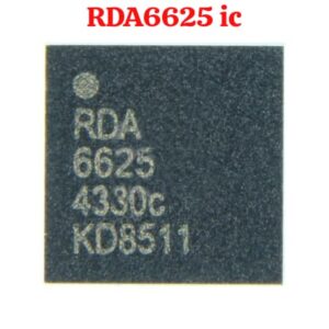
The RDA6625 is a high-performance, quad-band front-end module (FEM) specifically designed for mobile communication devices. It is most commonly found in feature phones and entry-level smartphones from brands like Huawei, Xiaomi, and various Honor models. RDA6625 Mobile Phone IC
This IC integrates high-efficiency power amplifiers (PA) with an antenna switch and a complete power control solution. It is built using an advanced GaAs HBT (Gallium Arsenide Heterojunction Bipolar Transistor) process for the power amplifiers and a CMOS process for the controller, ensuring a balance between high output power and energy efficiency. RDA6625 Mobile Phone IC
Technical Specifications
The following tables outline the mechanical, electrical, and functional parameters of the RDA6625.
1. General Product Specifications
| Feature | Specification |
| Manufacturer | RDA Microelectronics |
| Package Type | 32-pin LGA (Land Grid Array) |
| Package Size | $5\text{mm} \times 5\text{mm} \times 1.1\text{mm}$ |
| Frequency Bands | GSM850, EGSM900, DCS1800, PCS1900 |
| Process Technology | GaAs HBT / CMOS |
| Input/Output Impedance | $50\,\Omega$ (On-chip matched) |
| ESD Protection | Integrated at Antenna port |
2. Absolute Maximum Ratings
Exceeding these limits may cause permanent damage to the device.
| Parameter | Rating | Unit |
| Supply Voltage ($V_{CC}$) | -0.3 to +5.0 | V |
| Power Control Voltage ($V_{ramp}$) | -0.3 to +3.0 | V |
| Input RF Power | +10 | dBm |
| Operating Temperature | -30 to +110 | °C |
| Storage Temperature | -30 to +150 | °C |
| Maximum Duty Cycle | 50 | % |
3. Electrical Characteristics (RF Performance)
Typical values measured at $V_{CC} = 3.6\text{V}$ and $T = 25\text{°C}$.
| Parameter | Band | Min | Typ | Max | Unit |
| Frequency Range | GSM850/900 | 824 | – | 915 | MHz |
| DCS/PCS | 1710 | – | 1910 | MHz | |
| Output Power ($P_{out}$) | GSM850/900 | 33 | 33.5 | – | dBm |
| DCS/PCS | 30 | 30.5 | – | dBm | |
| Total Efficiency | GSM850/900 | 40% | – | – | – |
| DCS/PCS | 35% | – | – | – | |
| Supply Current | $P_{out} = \text{max}$ | – | 1.4 | – | A |
| Harmonics | $P_{out} \le 33\text{dBm}$ | – | -35 | -30 | dBm |
Pin Assignment and Configuration
The RDA6625 utilizes a 32-pin layout to handle RF inputs, outputs, and control logic.
| Pin Number | Pin Name | Description |
| 1–4, 8, 10–12, 15, 25, 27, 29–32 | GND | System Ground |
| 6 | RX2 | Receive Port 2 |
| 7 | RX3 | Receive Port 3 |
| 9 | ANT | Antenna Port (Matched to $50\,\Omega$) |
| 13, 14 | VCC | Main Power Supply (3.0V – 4.5V) |
| 16 | CTR1 | Control Logic Pin 1 |
| 17 | CTR0 | Control Logic Pin 0 |
| 18 | TXEN | Transmit Enable |
| 19 | RAMP | Power Ramp Control Pin |
| 20, 22 | CAP | External Capacitor Connection |
| 23 | DCSIN | DCS/PCS RF Input |
| 24 | GSMIN | GSM/EGSM RF Input |
| 5, 21, 26, 28 | NC | No Connection / Reserved |
Operational Logic (Truth Table)
The module’s mode of operation is determined by the logic states of the control pins.
| Mode | CTR1 | CTR0 | TXEN |
| Power Down | 0 | 0 | 0 |
| GSM Transmit | 0 | 0 | 1 |
| DCS Transmit | 1 | 0 | 1 |
| RX Port 2 | 1 | 0 | 0 |
| RX Port 3 | 1 | 1 | 0 |
Note: Logic “High” is typically $1.5\text{V}$ to $3.0\text{V}$, while Logic “Low” is $0\text{V}$ to $0.5\text{V}$.
Summary of Use Cases
The RDA6625 is a critical “Signal IC” or “Network IC.” Its primary role is to amplify the weak RF signals from the phone’s transceiver before they are sent out via the antenna, and to switch between transmit and receive modes rapidly. If your phone has “No Service” or “Searching” issues despite a valid SIM card, this IC is often the culprit in the repair process. RDA6625 Mobile Phone IC
More Products : https://gaffarmarketdelhi.com


