
S5525 Mobile Phone IC
High-Performance IC for Mobile Devices
The S5525 Mobile Phone IC is designed to deliver exceptional performance, ensuring smooth and reliable operation in a variety of mobile devices. Its advanced architecture allows for optimized power management, contributing to longer battery life and efficient energy usage. S5525 Mobile Phone IC
Compact and Durable Design
Engineered for durability and compact integration, the S5525 IC fits seamlessly into modern, sleek mobile phone designs. Its structure ensures reliability even in demanding applications, providing consistent results every time. S5525 Mobile Phone IC
Enhanced Compatibility and Versatility
The S5525 Mobile Phone IC is compatible with a range of devices and systems, making it a versatile choice for manufacturers. Whether you’re building high-end smartphones or cost-effective solutions, this IC supports a broad spectrum of applications with ease. S5525 Mobile Phone IC
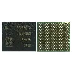
The S5525 IC (often listed as S5525 or SSMI S5525) is a specialized Radio Frequency (RF) integrated circuit used primarily in the front-end modules of modern smartphones. While it is most commonly found in Samsung Galaxy series devices (such as the A14, A34, M54, and older S-series), it is also utilized in some Motorola and mid-to-high-tier Android handsets. S5525 Mobile Phone IC
Its primary role is as an RF Transceiver or Network Power Amplifier (PA) Driver, responsible for managing the signal integrity between the phone’s antenna and the processor. S5525 Mobile Phone IC
Technical Specifications Table
| Feature | Detailed Specification |
| Component Name | S5525 / SSMI S5525-12 |
| Primary Function | RF Transceiver / Network Signal Processor |
| Device Category | RF Front-End Module (RFFE) |
| Manufacturer | Shenzhen SSMI Semiconductor (often OEM for Samsung) |
| Supported Networks | 2G (GSM), 3G (WCDMA), 4G (LTE), 5G (Sub-6GHz) |
| Package Type | LGA (Land Grid Array) or BGA (Ball Grid Array) |
| Pin Count | 48-Pin |
| Physical Dimensions | ~5mm x 5mm |
| Supply Voltage | 1.0V to 6.0V (Varies by power rail) |
| Operating Temperature | -40°C to +85°C |
| Max Peak Reflow Temp | 240°C – 260°C |
| Key Compatibility | Samsung Galaxy A14 5G, M54 5G, A34 5G, Moto G60 5G |
Core Functional Overview
The S5525 acts as the “translator” and “booster” for your phone’s wireless communications. It sits at the intersection of the digital logic and the physical antenna.
1. RF Transceiver Capabilities
The IC handles both the transmission (Tx) and reception (Rx) of radio waves. It converts digital data from the phone’s application processor into high-frequency analog signals that can be broadcast over cellular bands.
2. Multi-Band Support
One of the S5525’s strengths is its ability to handle a wide range of frequency bands. This is critical for 5G-enabled devices that must switch seamlessly between traditional LTE bands and newer 5G New Radio (NR) frequencies.
-
Low Bands: Better coverage and indoor penetration.
-
High/Mid Bands: Higher data speeds for streaming and downloads.
3. Signal Integrity and Power Management
Because mobile phones operate on limited battery power, the S5525 is designed with high efficiency. It manages Dissipation Power (typically around 0.6W) to ensure the device doesn’t overheat during long VoLTE calls or heavy data sessions.
Common Failure Symptoms
If the S5525 IC is damaged (often due to water ingress or physical drops), the phone will exhibit specific “Network” related issues:
-
“No Service” or “Emergency Calls Only”: The phone cannot register on the cellular network.
-
Weak Signal: The device shows 1 bar in areas where other phones have full reception.
-
Greyed-out Wi-Fi/Bluetooth: While primarily a cellular IC, in some integrated architectures, a failure here can destabilize the entire communication bus.
-
Rapid Battery Drain: A faulty RF IC may struggle to maintain a connection, causing the CPU to work overtime and drain the battery.
Repair & Technical Considerations
The S5525 is a Surface Mount Device (SMD). Replacing it requires professional-grade micro-soldering tools.
Important Note: This IC uses a Lead-Free (RoHS) solder profile. When replacing it, technicians must use a hot air station set precisely between 250°C and 300°C to avoid warping the multi-layered PCB of the smartphone.
Verification Before Installation:
-
Marking Check: Ensure the IC has the “S5525” or “S55255-12” laser-etched marking.
-
Pin Alignment: Check that the 48 pads on the underside are clean and uniform.
-
Impedance Test: Technicians often check for a short to ground on the VCC rail before powering the device after a replacement.
More Products : https://gaffarmarketdelhi.com


