

SR 3532S Mobile Phone IC
Streamlined Performance for Mobile Devices
Designed with precision, the SR 3532S Mobile Phone IC optimizes your device’s processing capabilities. Tailored for modern smartphones, this integrated circuit ensures seamless functionality, boosting speed and efficiency to enhance user experience. SR 3532S Mobile Phone IC
Compact and Reliable Design
Whether you are developing a new device or upgrading an existing one, the SR 3532S offers a compact design without compromising on power. Its advanced architecture makes it a reliable choice for high-performance mobile applications. SR 3532S Mobile Phone IC
Energy Efficiency for Extended Usability
Experience unmatched energy efficiency with the SR 3532S Mobile Phone IC. It significantly reduces power consumption, enabling extended device usability while maintaining performance standards.
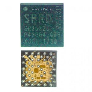
The SR3532S is a highly specialized Integrated Circuit (IC) developed by Spreadtrum Communications (now UNISOC).1 It is primarily categorized as an RF Transceiver or Intermediate Frequency (IF) IC, specifically designed for mobile communication devices.2
In mobile hardware architecture, the SR3532S serves as a critical bridge between the baseband processor and the antenna, handling the modulation and demodulation of signals. It gained significant prominence for its use in Samsung’s Tizen-based smartphones (like the Samsung Z3) and various entry-level Android devices. SR 3532S Mobile Phone IC
SR3532S Technical Specifications
The following table outlines the core technical parameters of the SR3532S IC.
| Feature | Specification Details |
| Manufacturer | Spreadtrum Communications (UNISOC) |
| IC Type | RF Transceiver / Intermediate Frequency (IF) IC |
| Package Type | BGA (Ball Grid Array) / QFN (Quad Flat No-lead) |
| Pin Count | 20-Pin (Standard Variant) / 50-Pin (BGA Variant) |
| Supported Networks | WCDMA (3G), GSM (2G), GPRS/EDGE |
| Operating Voltage | $2.7V$ to $5.5V$ |
| Frequency Range | 50Hz (Baseband Interface) to Multi-band RF |
| Operating Temp | $-40\text{°C}$ to $+85\text{°C}$ |
| Typical Power | ~8W (Peak Audio/RF Output combined) |
| Application | Smartphones, Feature Phones, IoT Modules |
Key Functional Components
To understand how the SR3532S operates within a mobile phone, it is helpful to look at its functional blocks.
1. RF Transceiver Logic
The SR3532S acts as a “translator.” It takes the low-frequency digital data from the phone’s CPU and converts it into high-frequency radio waves for transmission. Conversely, it receives weak incoming radio signals and converts them into a format the processor can understand. SR 3532S Mobile Phone IC
2. Intermediate Frequency (IF) Processing
The “S” in the SR3532S series often denotes specific refinements in IF handling. By processing signals at an intermediate frequency before final conversion, the IC minimizes noise and interference, ensuring a stable call connection even in areas with weak signal strength. SR 3532S Mobile Phone IC
3. Power Management Integration
While primarily an RF chip, it includes specialized power-saving states. In mobile devices, the radio is one of the largest “battery killers.” The SR3532S utilizes an optimized sleep mode that draws minimal current when the phone is not actively transmitting data. SR 3532S Mobile Phone IC
Common Use Cases and Repairs
The SR3532S is a common component in the repair industry. Because it handles the physical connection to the cellular network, it is often the first part to fail if a phone suffers from:
-
“No Service” or “Searching” errors despite a valid SIM card.
-
Weak signal reception compared to other devices.
-
Overheating during long phone calls or heavy data usage.
Compatibility Table
| Device Model | Role of SR3532S |
| Samsung Z3 (Tizen) | Primary RF Transceiver |
| Samsung Galaxy J1/J2 | Network Signal Processor |
| Spreadtrum SoC Kits | Reference RF Design |
Technical Note for Technicians
When replacing this IC, professionals must use a BGA Reballing technique. The chip is sensitive to heat; excessive temperature during soldering (typically above 260°C) can damage the internal silicon layers. It is highly recommended to use a high-quality flux and a controlled hot air station to ensure all 20 or 50 pins make a perfect connection with the PCB (Printed Circuit Board).
More Products : https://gaffarmarketdelhi.com


